Bottom pinned SOT-MRAM bit structure and method of fabrication

a sot-mram and bottom-pinned technology, applied in the direction of magnetic field-controlled resistors, digital storage, instruments, etc., can solve the problems of large amount of current required for switching the state of the cell, the mtj memory elements of the stt-mram device suffer from wear-effects, and the current technology may not be able to meet the current and future capacity demands of next-generation computing systems, etc., to achieve large spin-orbit coupling strength

Active Publication Date: 2017-09-19
WESTERN DIGITAL TECH INC
View PDF11 Cites 17 Cited by
  • Summary
  • Abstract
  • Description
  • Claims
  • Application Information

AI Technical Summary

Benefits of technology

[0009]Embodiments of the present disclosure generally relate to data storage and computer memory systems, and more particularly, to a SOT-MRAM chip architecture. The SOT-MRAM chip architecture includes a plurality of leads, a plurality of memory cells, and a plurality of transistors. The leads may be made of a material having large spin-orbit coupling strength and high electrical resistivity. Each individual lead may include a plurality of first portions and a plurality of second portions distinct from the first portions. The electrical resistivity of the second portions is less than that of the first portions, so the total electrical resistivity of the lead is reduced, leading to improved power efficiency and signal to noise ratio.

Problems solved by technology

Today the memory technologies that generally dominate the computing industry are DRAM and NAND flash; however these memory technologies may not be able to address the current and future capacity demands of next generation computing systems.
However, the MTJ memory elements in STT-MRAM devices suffer from wear-effects due to driving a sufficient amount of current for switching through the MTJ, including through the barrier layer.
Typically, a large amount of current is required for switching the state of the cell.
Over time, the barrier layer breaks down due to the large amount of current, rendering the MTJ useless.

Method used


Image

  • Bottom pinned SOT-MRAM bit structure and method of fabrication
  • Bottom pinned SOT-MRAM bit structure and method of fabrication
  • Bottom pinned SOT-MRAM bit structure and method of fabrication

Examples


Embodiment Construction

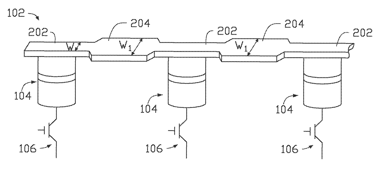
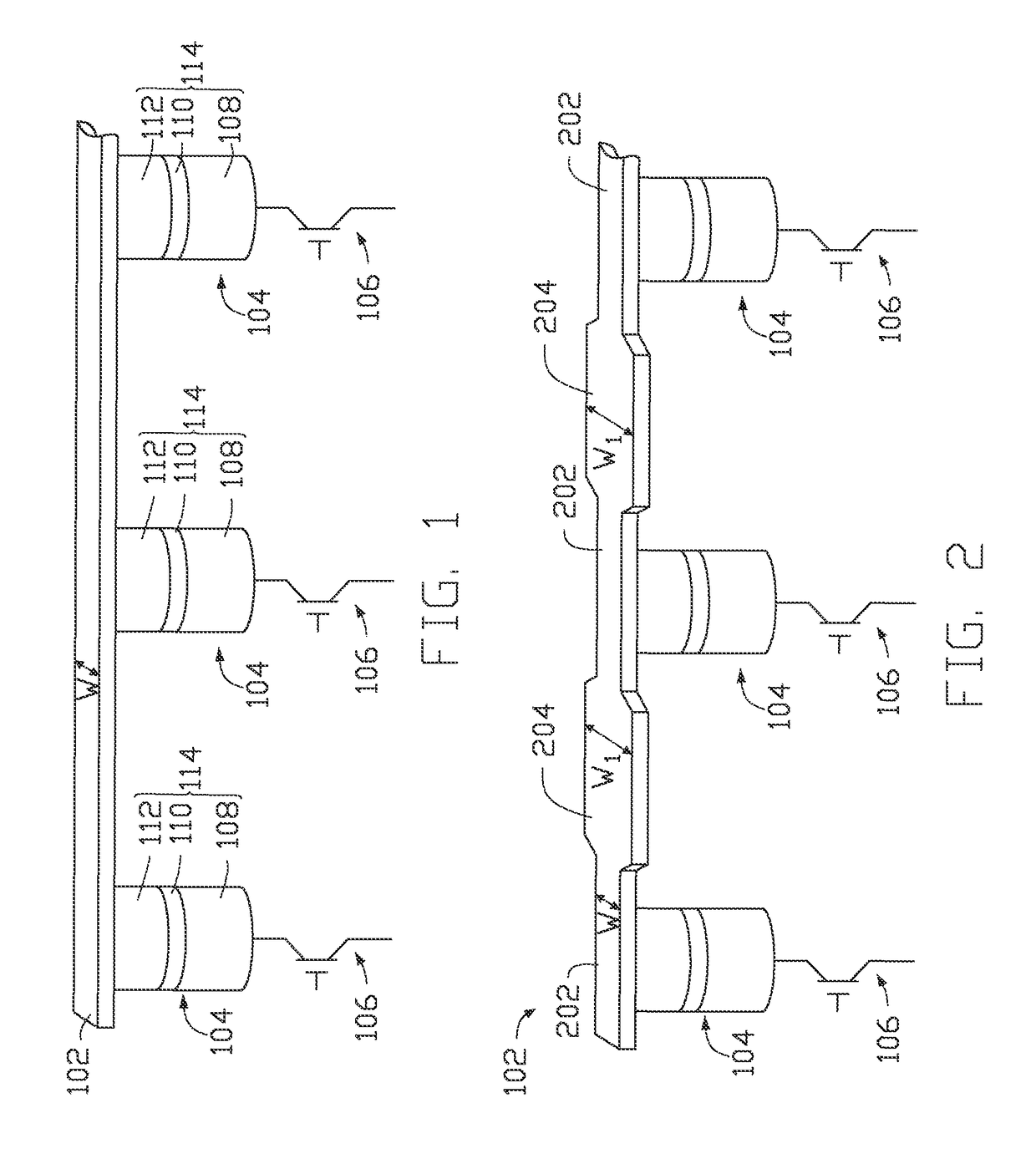
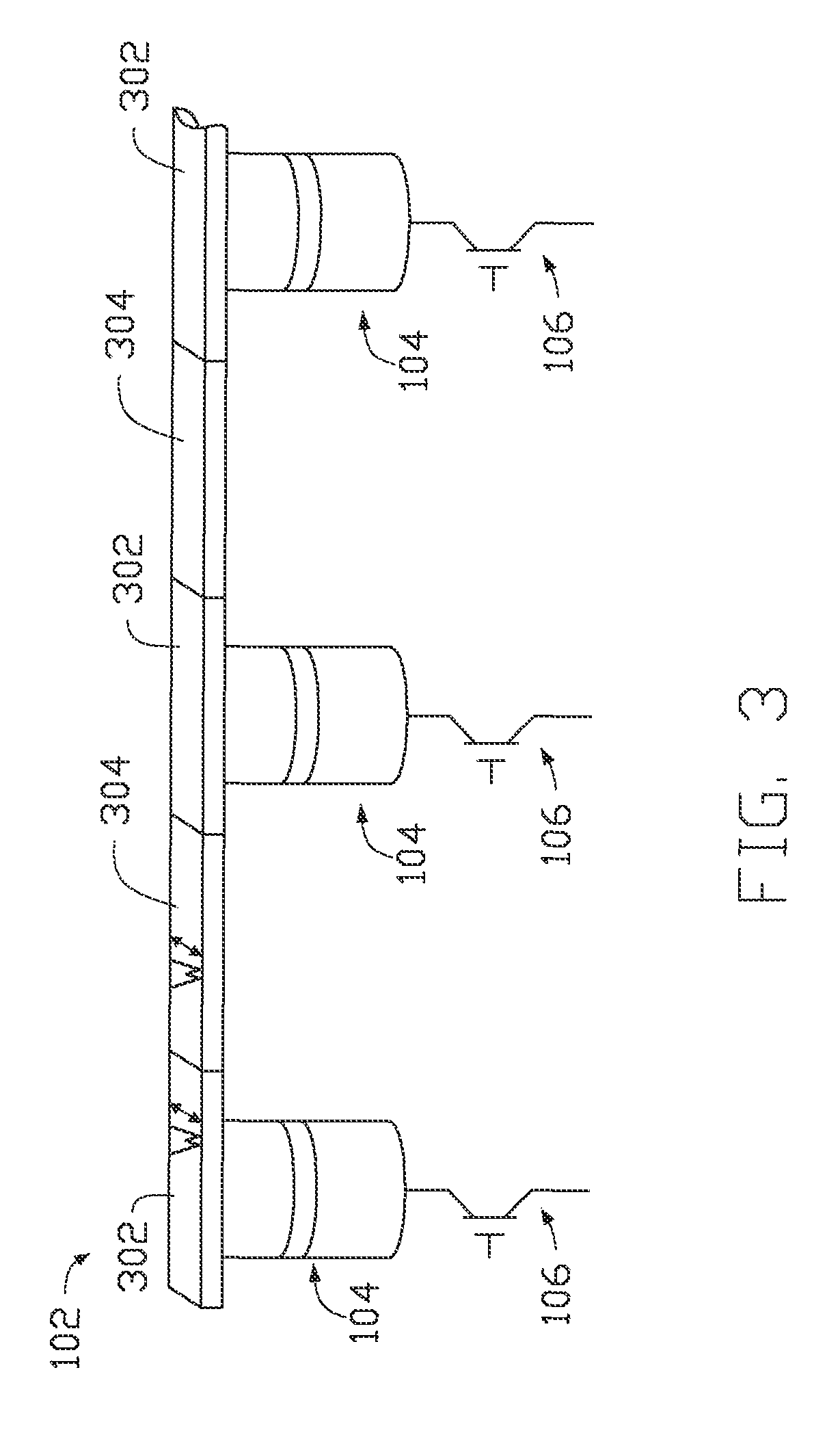
[0021]In the following, reference is made to embodiments of the disclosure. However, it should be understood that the disclosure is not limited to specific described embodiments. Instead, any combination of the following features and elements, whether related to different embodiments or not, is contemplated to implement and practice the disclosure. Furthermore, although embodiments of the disclosure may achieve advantages over other possible solutions and / or over the prior art, whether or not a particular advantage is achieved by a given embodiment is not limiting of the disclosure. Thus, the following aspects, features, embodiments and advantages are merely illustrative and are not considered elements or limitations of the appended claims except where explicitly recited in a claim(s). Likewise, reference to “the disclosure” shall not be construed as a generalization of any inventive subject matter disclosed herein and shall not be considered to be an element or limitation of the ap...


PUM


Abstract

Embodiments of the present disclosure generally relate to data storage and computer memory systems, and more particularly, to a SOT-MRAM chip architecture. The SOT-MRAM chip architecture includes a plurality of leads, a plurality of memory cells, and a plurality of transistors. The leads may be made of a material having large spin-orbit coupling strength and high electrical resistivity. Each lead of the plurality of leads may include a plurality of first portions and a plurality of second portions distinct from the first portions. The electrical resistivity of the second portions is less than that of the first portions, so the total electrical resistivity of the lead is reduced, leading to improved power efficiency and signal to noise ratio.

Description

BACKGROUND OF THE DISCLOSURE[0001]Field of the Disclosure[0002]Embodiments of the present disclosure generally relate to data storage and computer memory systems, and more particularly, to a spin-orbit torque magnetoresistive random access memory (SOT-MRAM) chip architecture.[0003]Description of the Related Art[0004]The heart of a computer is a magnetic recording device which typically may include a rotating magnetic media or a solid state media device. A number of different memory technologies exist today for storing information for use in a computing system. These different memory technologies may, in general, be split into two major categories: volatile memory and non-volatile memory. Volatile memory may generally refer to types of computer memory that require power to retain stored data. Non-volatile memory, on the other hand, may generally refer to types of computer memory that do not require power in order to retain stored data. Examples of volatile memory may include certain ...

Claims


Application Information

Patent Timeline
Patent Type & Authority Patents(United States)
IPC IPC(8): G11C11/00H01L43/08H01L43/02G11C11/16H01L27/22H01L43/12
CPCH01L27/228G11C11/161G11C11/1675H01L43/02H01L43/08H01L43/12G11C11/18H10B61/22G11C11/1659H01L28/00H10N50/85H10N50/01H10N50/10H10B43/27H10N50/80
Inventor BRAGANCA, PATRICK M.TSENG, HSIN-WEIWAN, LEI
Owner WESTERN DIGITAL TECH INC
Why Eureka
Try Eureka