
Method and apparatus for fully integrating a voltage controlled oscillator on an integrated circuit

a voltage control and integrated circuit technology, applied in the direction of discrete pretuned circuits, pulse techniques, pulse generators, etc., can solve the problems of difficult and costly implementation of tuned networks or circuits using on-chip passive electrical components, poor tolerance values of integrated circuit components, and low tolerance values of passive circuit components

Inactive Publication Date: 2001-07-31
CSR TECH INC
View PDF14 Cites 83 Cited by
  • Summary
  • Abstract
  • Description
  • Claims
  • Application Information

AI Technical Summary

Benefits of technology

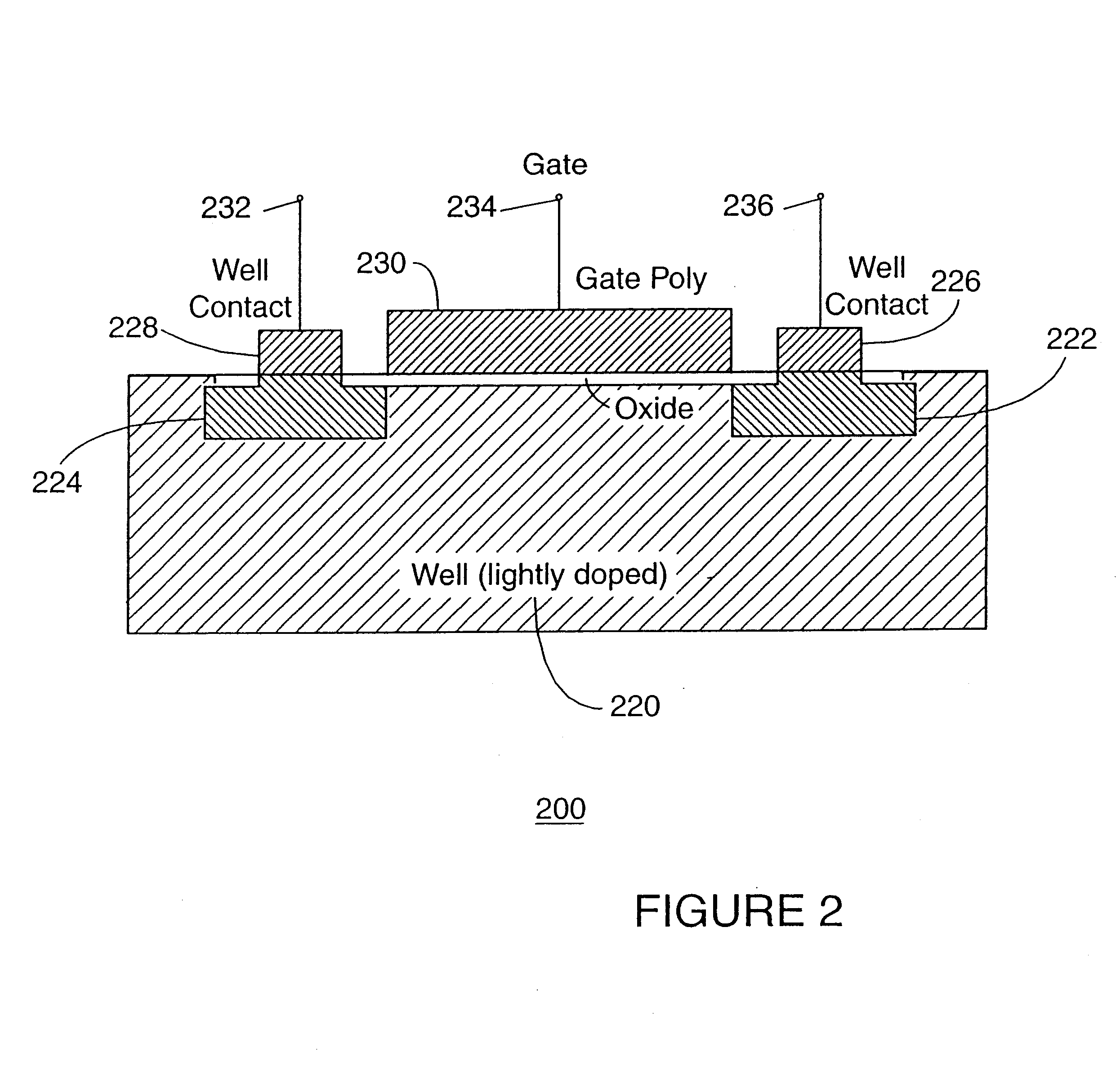
The analog tuning varactor preferably comprises an integrated circuit varactor structure having a wide tuning capacitance range. The IC varactor structure preferably includes either a P-gate / N-well or N-gate / P-well layer structure ideally formed on a Silicon On Insulator (SOI) substrate. The tuning varactor is preferably completely isolated from the IC substrate by an oxide layer of the SOI substrate and by oxide-filled trenches formed on both sides of the varactor structure. The trenches preferably extend to the oxide layer of the SOI substrate. Owing to the lack of a junction between the well and the substrate, the tuning varactor introduces reduced parasitic capacitance into the IC, and what capacitance is introduced is linear. Consequently, the analog tuning varactor reduces the sensitivity of the VCO to low frequency energy occurring in the IC substrate. The tuning varactor also provides an improved tuning capacitance range, which, in turn, increases the frequency tuning range of the fully integrated VCO. The tuning varactor preferably slowly changes from a lower capacitance value to a higher capacitance value.
The VCO high Q inductors preferably comprise inductors having high Q values, high self-resonance, and low loss integrated circuit inductors that reduce the LO radiation introduced into the IC substrate. The IC inductors are preferably formed on an SOI substrate where the substrate of the SOI preferably has a high resistivity. The high Q inductor structure preferably includes a shielding pattern that induces a plurality of small eddy currents to shield the IC substrate from magnetic energy generated by the inductor. The inductor has a high quality factor and a high self-resonance frequency due to the effective shielding of electromagnetic energy from the IC substrate while not reducing the effective inductance of the inductor or introducing substantial parasitic capacitance. This, in turn, improves the overall performance of the fully integrated VCO, increases the VCO tuning range, makes the VCO more reliable and useful in a wider variety of applications such as in mixed signal environments, and aids in reducing the VCO noise sensitivity.
By virtue of improved performance characteristics provided by the digital capacitor, the analog tuning varactor, the high Q inductor, and the trench isolated guard ring, the inventive VCO can be fully integrated despite poor tolerance values typically associated with process variations in integrated circuit fabrication. The present invention improves the performance of wireless communication devices without requiring the use of expensive and large discrete components. The present invention is particularly useful in broadband wireless digital communication systems such as CDMA cellular systems, however it can also find utility in other communication systems such as those made in accordance with the proposed Bluetooth standard.

Problems solved by technology

One well-known problem to those skilled in the art of the design and manufacture of integrated circuits is the poor tolerance values associated with integrated circuit components, especially the tolerance values of passive circuit components.
Consequently, it has proven difficult and costly in the past to implement tuned networks or circuits using on-chip passive electrical components.
Disadvantageously, the trimming techniques produce only static solutions.
For example, in fuse trimming, although the devices may perform adequately under nominal conditions, they may not perform adequately under all of the operating conditions of the integrated circuit.
However, disadvantageously, the integrated circuit is permanently configured once the fuses are blown.
Devices that were once usable under the nominal conditions at which the fuses were blown may become unusable under some operating conditions, thus adversely affecting yield characteristics of the integrated circuits.
In addition, the prior art post-fabrication solutions disadvantageously introduce additional manufacturing and testing steps into the manufacturing process.
Thus, the prior art post-fabrication trimming techniques add additional time to the design and fabrication of integrated circuit devices and consequently add to the manufacturing costs of the integrated circuits.
Disadvantageously, when the VCO is implemented in an integrated circuit, poor tolerance values due to IC fabrication process variations and other factors can adversely affect the previously tuned center frequency.
Consequently, the prior art VCO integrated circuit implementations disadvantageously require calibration to re-center the LC-resonator circuit's resonance frequency to a desired center frequency value.
Due to variations from part to part, the prior art IC VCO implementations may be unreliable and totally unusable, especially when operating at high frequencies.
This limitation in the prior art IC VCO implementations also disadvantageously limits the frequency range over which the VCO can be tuned (the VCO tuning range).
However, due to process variations and other factors, the tuning ranges of the prior art IC VCO implementations are limited even further.
In addition to variations in desired center frequencies, the prior art IC VCO implementations disadvantageously are also very sensitive to low frequency noise that is introduced into the IC substrate.
This sensitivity to noise characteristic not only further limits the prior art VCO tuning ranges, but it also severely limits the utility of the prior art VCO designs in some important applications, such as use in a mixed signal (analog and digital) integrated circuit environment.
This non-linear well-substrate junction capacitance is particularly problematic in IC VCO implementations.
Furthermore, due to the well-substrate junction of prior art designs, the total parasitic capacitance is also increased.
Increased parasitic capacitance disadvantageously also decreases the tuning range of the IC VCO implementations.
Consequently, due to the well-substrate junctions of the prior art IC VCO designs, the VCO center output frequencies have proven unreliable from part to part, and they also are not amenable for use in a mixed signal environment.
Low frequency noise caused by digital circuitry located elsewhere on the integrated circuit disadvantageously is introduced into the substrate and propagates through the substrate to the VCO, whereat it FM-modulates the VCO center output frequency.
This renders these prior art IC VCO designs useless for some applications where the center output frequency must be tightly controlled such as in wireless communication systems.
Disadvantageously, these junction diode tuning varactors also introduced parasitic capacitance into the VCO circuits.
In addition, the traditional varactors were limited in that they could only change capacitance values by at most a factor of 1 / 2 per octave, which, in turn, caused the tuning range of the VCO to be limited to a factor of 1 / 2 per octave.
The prior art tuning varactors therefore further limited the tuning range of the VCO.
In addition, the prior art VCO designs disadvantageously create a forward bias conduction of current that is applied to the varactors due to the large swings experienced by the prior art VCO designs.
Disadvantageously, the forward bias conduction of current reduces the effective Q of the tank circuit in the VCO.
Low Q values of the inductors produce increases in phase noise and frequency errors.
In addition, for the reasons provided above, the inductors also add parasitic capacitance to the IC due to the existence of low-resistivity substrates used in the prior art implementations.
Further, the local oscillation (LO) radiation produced by the prior art inductors disadvantageously radiate down into the IC substrate and thereby introduce undesirable noise energy into the substrate.
Not only does this detrimentally affect the performance of the VCO (by further limiting the tuning range), the radiated noise energy detrimentally affects other circuits in the IC.
This can be especially detrimental in a mixed signal IC.
The inductors in the prior art IC VCO designs consequently further limited the performance, utility, and tuning range of the prior art IC VCO implementations.
Consequently, the analog tuning varactor reduces the sensitivity of the VCO to low frequency energy occurring in the IC substrate.
However, any noise present on the analog control line will FM-modulate the VCO output frequency.
However, it will not significantly FM-modulate the VCO output frequency.
Disadvantageously, when the VCO is implemented in an integrated circuit, poor tolerance values due to IC fabrication process variations and other factors can adversely affect the desired tuned center frequency.
Consequently, the prior art IC VCO disadvantageously are unreliable due to variations between integrated circuits.
In addition, as described above, use of the analog tuning varactor for fine-tuning the output frequency of the VCO also reduces the VCO noise sensitivity.

Method used


Image

  • Method and apparatus for fully integrating a voltage controlled oscillator on an integrated circuit
  • Method and apparatus for fully integrating a voltage controlled oscillator on an integrated circuit
  • Method and apparatus for fully integrating a voltage controlled oscillator on an integrated circuit

Examples


Embodiment Construction

of the Fully-Integrated VCO of the Present Invention

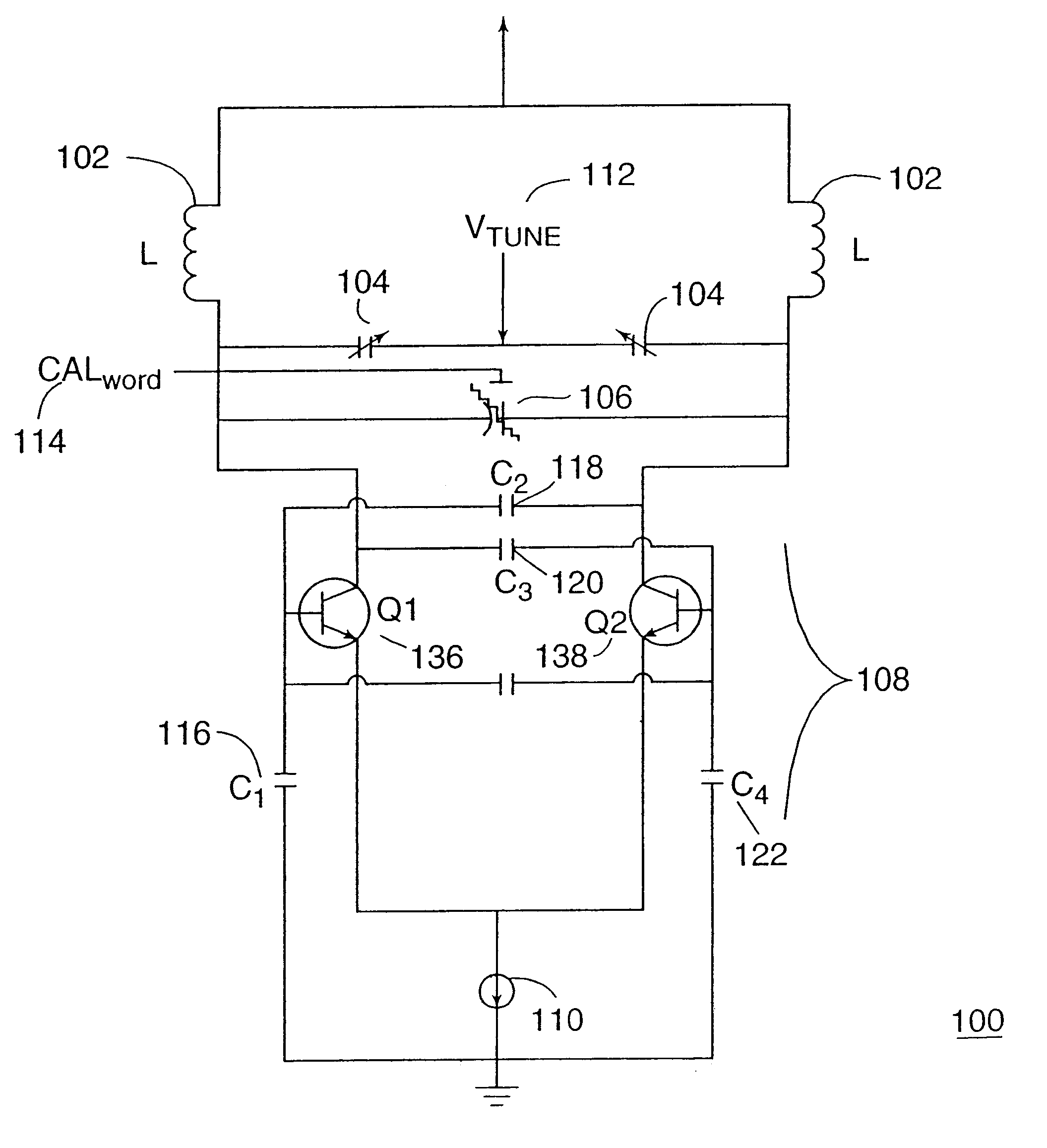
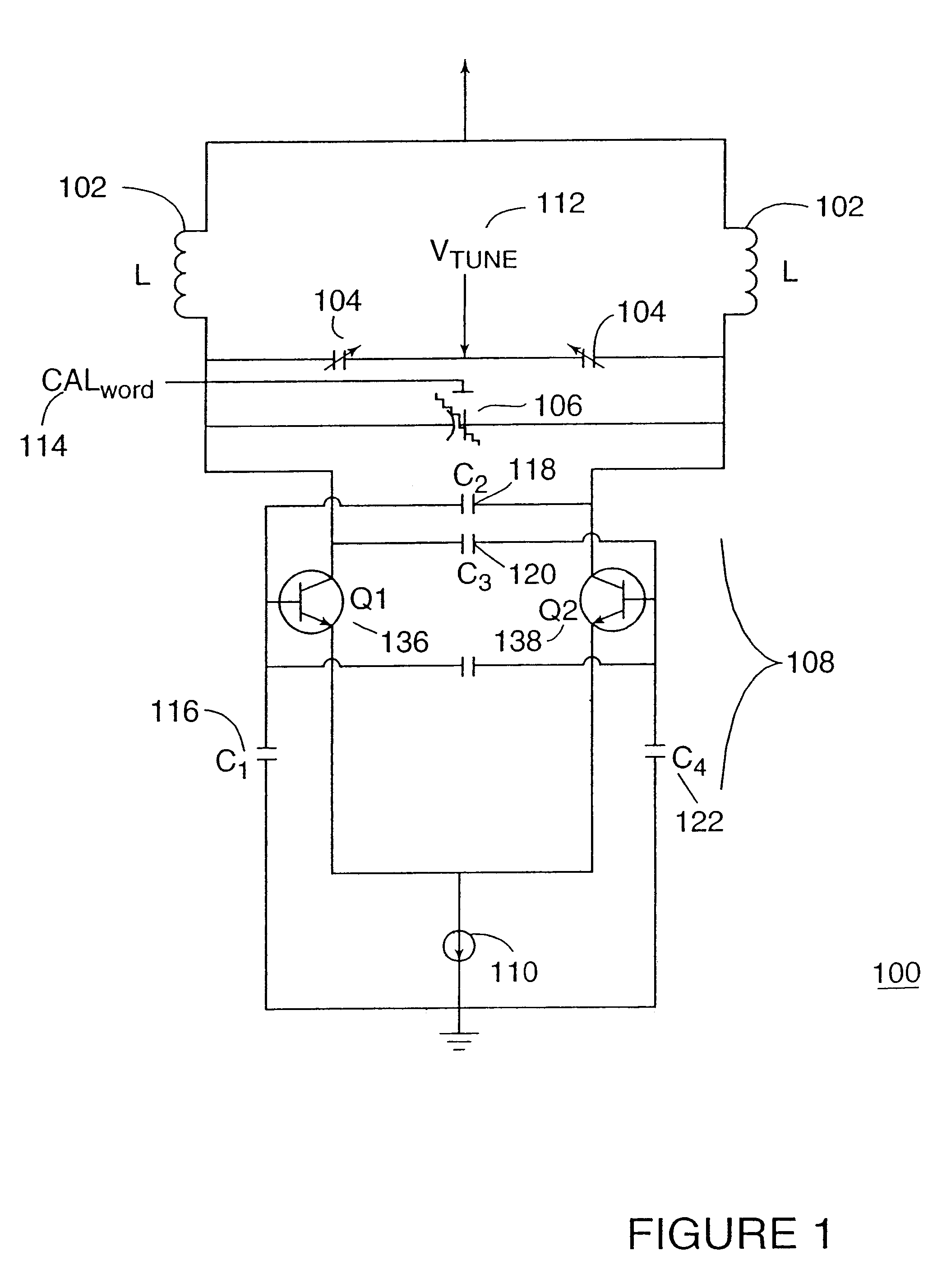
FIG. 7 shows a detailed schematic of the preferred integrated VCO 100 of FIG. 1. In the embodiment of the VCO 100 shown in FIG. 7, the VCO 100 preferably comprises a pair of high Q inductors 102 and 102', two pairs of analog tuning varactors 104, a multi-bit digital capacitor 106, a differential pair amplifier 108, a current source 110, feedback and bias capacitors 116, 118, 120, and 122, bias circuitry 130, and output buffer circuitry 132. The inductors L.sub.1 102 and L.sub.2 102' preferably comprise high Q inductors as described in detail above with reference to FIG. 1. As described above with reference to FIG. 1, the analog tuning varactors 104 are preferably controlled by an analog tuning voltage V.sub.tune 112. In the embodiment shown in FIG. 7, the VCO 100 uses two differential analog tuning varactors 104. Two differential tuning varactors 104 are used in the embodiment shown to permit access to two tuning control ports at V...


PUM


Abstract

A method and apparatus for fully integrating a Voltage Controlled Oscillator (VCO) on an integrated circuit. The VCO is implemented using a differential-mode circuit design. The differential-mode implementation of the VCO preferably comprises a differential mode LC-resonator circuit, a digital capacitor, a differential pair amplifier, and a current source. The LC-resonator circuit includes at least one tuning varactor and two high Q inductors. The tuning varactor preferably has a wide tuning capacitance range. The tuning varactor is only used to "fine-tune" the center output frequency f0 of the VCO. The center output frequency f0 is coarsely tuned by the digital capacitor. The VCO high Q inductors comprise high gain, high self-resonance, and low loss IC inductors. The IC VCO is fabricated on a high resistivity substrate material using a trench isolated guard ring. The guard ring isolates the fully integrated VCO, and each of its component parts, from RF signals that may be introduced into the IC substrate by other devices. By virtue of the improved performance characteristics provided by the digital capacitor, the analog tuning varactor, the high Q inductor, and the trench isolated guard ring techniques, the inventive VCO is fully integrated despite process variations in IC fabrication.

Description

1. Field of the InventionThis invention relates to integrated circuit devices, and more particularly to a method and apparatus for fully integrating a Voltage Controlled Oscillator (VCO) on an Integrated Circuit (IC) device.2. Description of Related ArtOne well-known problem to those skilled in the art of the design and manufacture of integrated circuits is the poor tolerance values associated with integrated circuit components, especially the tolerance values of passive circuit components. Due to process variations, device parameter spread, variations in critical parameters such as conductive layer sheet resistance values, film thickness, process uniformity and manufacturing equipment cleanliness, and other factors, integrated circuit passive electrical components often have tolerances that are approximately an order of magnitude worse than their analogous discrete external passive electrical components. Consequently, it has proven difficult and costly in the past to implement tune...

Claims


Application Information

Patent Timeline
Patent Type & Authority Patents(United States)
IPC IPC(8): H03J5/24H03B7/06H03B7/00H03J5/00H03B5/12H03B5/08
CPCH03B7/06H03J5/246H03B5/1246H03B5/1215H03B5/1243H03B5/1231H03J2200/10
Inventor MUCKE, LARS HENRIKHULL, CHRISTOPHER DENNISJANSSON, LARS GUSTAF
Owner CSR TECH INC
Learn More