Semiconductor Device with Heterojunctions and an Inter-Finger Structure

a technology of heterojunction and semiconductor, applied in the direction of photovoltaic energy generation, electrical equipment, climate sustainability, etc., can solve the problems of high thermal budget used during the production process, unsuitable for obtaining low-cost solar cells, and high cost of materials

Inactive Publication Date: 2008-03-13
COMMISSARIAT A LENERGIE ATOMIQUE ET AUX ENERGIES ALTERNATIVES
View PDF22 Cites 80 Cited by
  • Summary
  • Abstract
  • Description
  • Claims
  • Application Information

AI Technical Summary

Benefits of technology

[0020] In addition, the dielectric regions between the amorphous regions extend to the substrate, ensuring both the electrical insulation between the amorphous regions and the passivation of the substrate surface, providing a simpler structure and better electrical insulation between the amorphous semiconductor regions than the existing devices.
[0023] It is also possible for at least one first conductive thermal oxide area to be located between the first metallization area and the first amorphous semiconductor region and for at least one second conductive thermal oxide area to be located between the second metallization area and the second amorphous semiconductor region. These conductive thermal oxide areas make it possible to provide better contact resistivity between the metallization areas and the amorphous semiconductor regions.
[0026] The semiconductor substrate can comprise on another surface, opposite the surface having the interdigitated structure, a surface passivation layer coated with an antireflective layer. The surface passivation layer makes it possible to push away the current carriers, and the antireflective layer makes it possible to trap the maximum number of photons entering the device.
[0030] It is possible for the first and / or the second amorphous semiconductor region to be doped gradually, so as to provide a good interface with the semiconductor substrate.
[0035] Intrinsic semiconductor regions can be placed between the amorphous semiconductor regions and the substrate, making it possible to provide a good interface with the substrate and preventing recombinations at the level of the substrate.
[0064] Thus, the metallization areas are used as a mask to carry out the etching of the amorphous semiconductor layers. This method is simple and inexpensive to implement because the etching steps require only a simple alignment with respect to the metallization areas in order to be implemented.

Problems solved by technology

The major disadvantage of this type of structure, in particular in the production of solar cells, is the high thermal budget used during the production process.
However, this type of material is usually very expensive, and therefore unsuitable for obtaining low-cost solar cells.
However, using such a production process with a high thermal budget leads to considerable thermal stress in the material, and therefore increases the risk of damage in the production process.
The major disadvantage of these heterojunction cells is that there is only one possible connection structure: an electrode on the amorphous silicon side and an electrode on the crystalline silicon side.
In this device, the electrical insulation and the surface passivation require two different layers because the material of the insulating layer is unsuitable for surface passivation.

Method used


Image

  • Semiconductor Device with Heterojunctions and an Inter-Finger Structure
  • Semiconductor Device with Heterojunctions and an Inter-Finger Structure
  • Semiconductor Device with Heterojunctions and an Inter-Finger Structure

Examples


Embodiment Construction

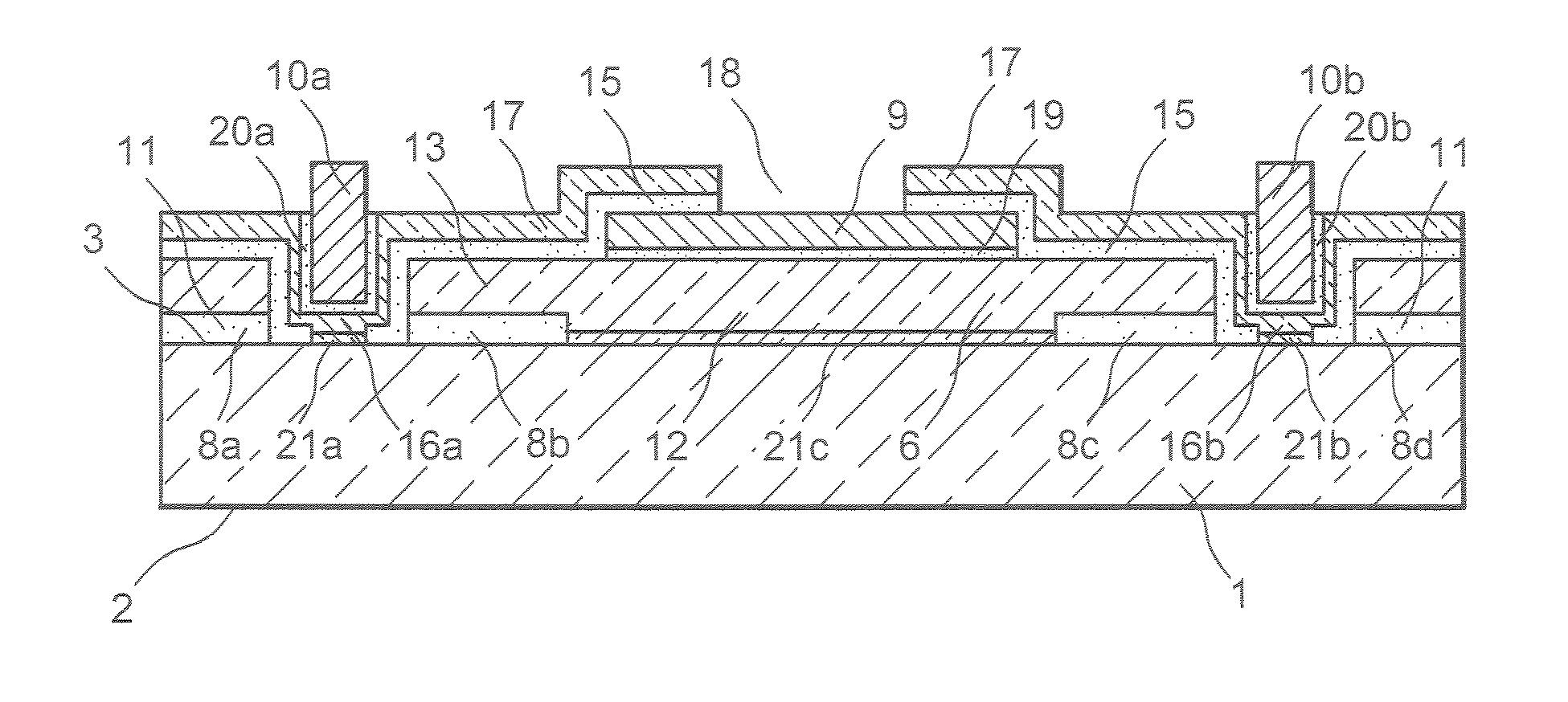
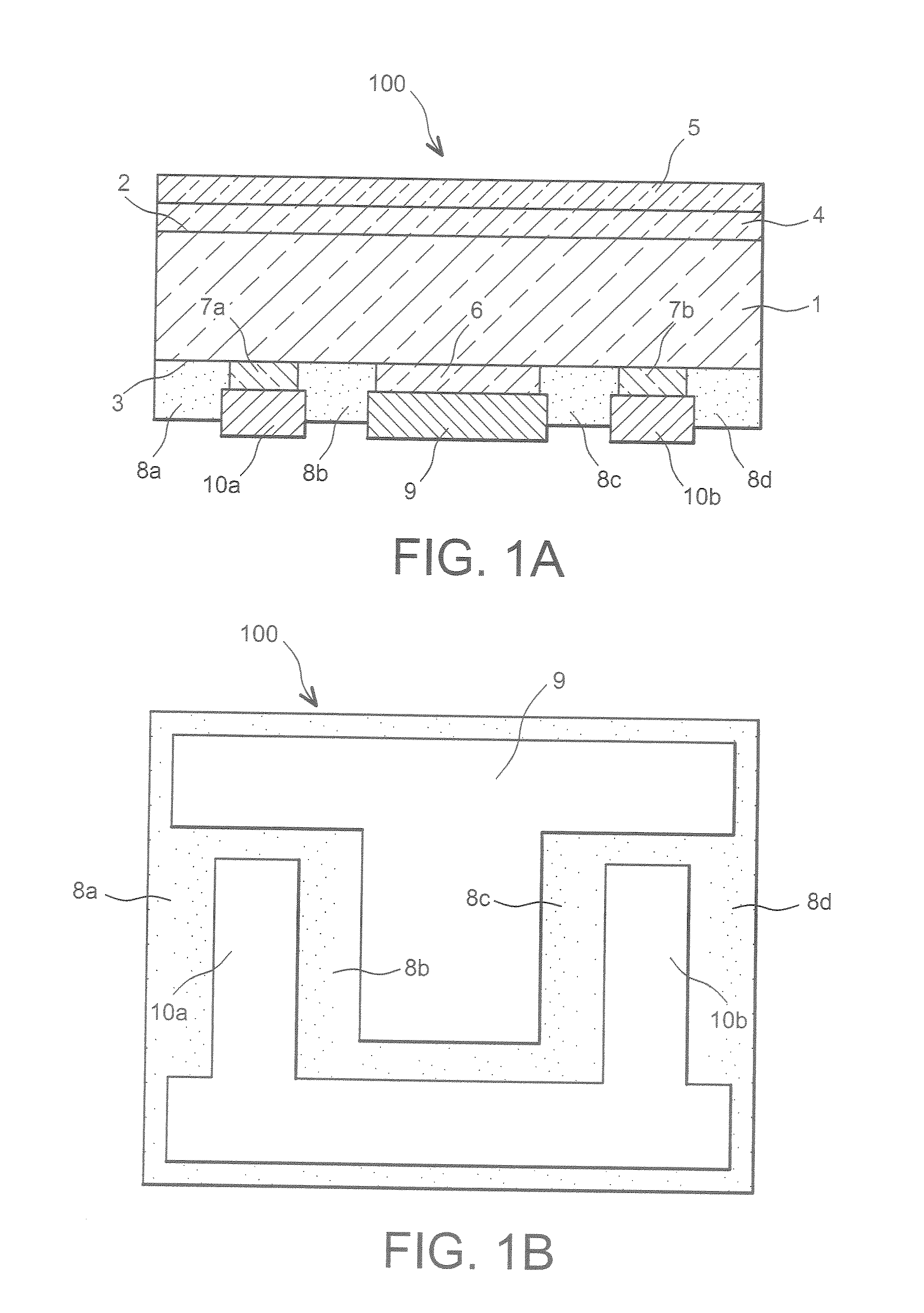
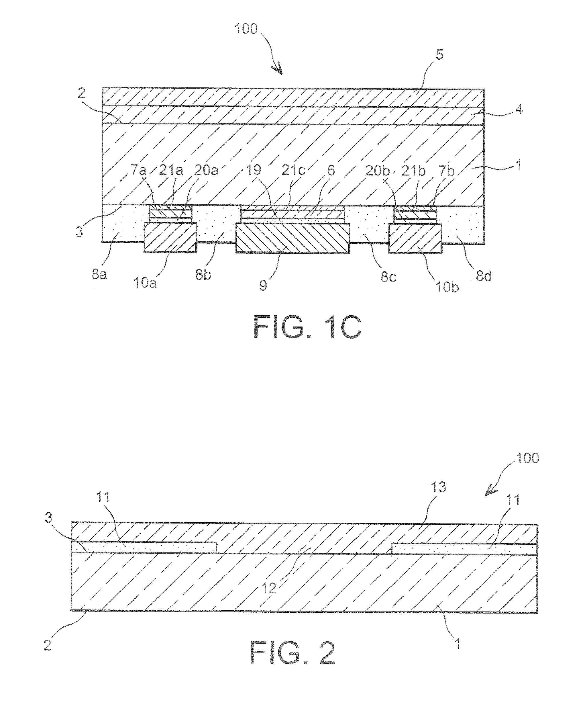
[0017] This invention is intended to propose a semiconductor device with heterojunctions, which does not have the disadvantage mentioned above, namely that of being limited by a connection structure including an electrode on two main opposite surfaces of the device, and which proposes a simpler and more electrically-insulated structure than the existing semiconductor devices with an interdigitated structure.

[0018] To achieve these objectives, this invention proposes a semiconductor device comprising, on at least one surface of a crystalline semiconductor substrate, at least one first amorphous semiconductor region doped with a first type of conductivity, which semiconductor substrate comprises, on the same surface, at least one second amorphous semiconductor region doped with a second type of conductivity, opposite the first type of conductivity, wherein the first amorphous semiconductor region, insulated from the second amorphous semiconductor region by at least one dielectric reg...


PUM


Abstract

A semiconductor device including, on at least one surface of a crystalline semiconductor substrate, at least one first amorphous semiconductor region doped with a first type of conductivity. The semiconductor substrate includes, on the same at least one surface, at least one second amorphous semiconductor region doped with a second type of conductivity, opposite the first type of conductivity. The first amorphous semiconductor region, insulated for the second amorphous semiconductor region by at least ore dielectric region in the contact with the semiconductor substrate, and the second amorphous semiconductor region form an interdigitated structure.

Description

TECHNICAL FIELD [0001] This invention relates to a semiconductor device with heterojunctions and an interdigitated structure placed on a semiconductor layer of the device, at to the method for production thereof. Such a device can be, for example, a solar cell having an interdigitated structure integrating heterojunctions, and the method is particularly suitable for producing this type of solar cell, on thin-layer silicon. PRIOR ART [0002] Various technologies are currently used to produce semiconductor devices. In the production of solar cells, two types of technology are primarily used: homojunction cells and heterojunction cells. [0003] The patent U.S. Pat. No. 4,234,352 describes a homojunction solar cell with an interdigitated structure. This cell comprises a crystalline silicon substrate. This substrate has two opposite surfaces. One of the surfaces, called the front surface, is intended to receive light, while the other surface comprises a plurality of N- or P-doped regions. ...

Claims


Application Information

Patent Timeline
Patent Type & Authority Applications(United States)
IPC IPC(8): H01L29/04H01L21/02H01L31/0745H01L31/0747
CPCH01L31/022433H01L31/0288H01L31/03529H01L31/0747H01L31/202Y02E10/50H01L31/022441H01L31/0745Y02P70/50
Inventor RIBEYRON, PIERRE JEANJAUSSAUD, CLAUDE
Owner COMMISSARIAT A LENERGIE ATOMIQUE ET AUX ENERGIES ALTERNATIVES
Why Eureka
Try Eureka