

Voltage regulator and semiconductor device
a voltage regulator and semiconductor technology, applied in the direction of electric variable regulation, process and machine control, instruments, etc., can solve the problem of limited driving of the nmos transistor 602/b>, and achieve the effect of not limiting the driving of the output transistor
- Summary
- Abstract
- Description
- Claims
- Application Information
AI Technical Summary
Benefits of technology
Problems solved by technology
Method used
Image

Examples
first embodiment
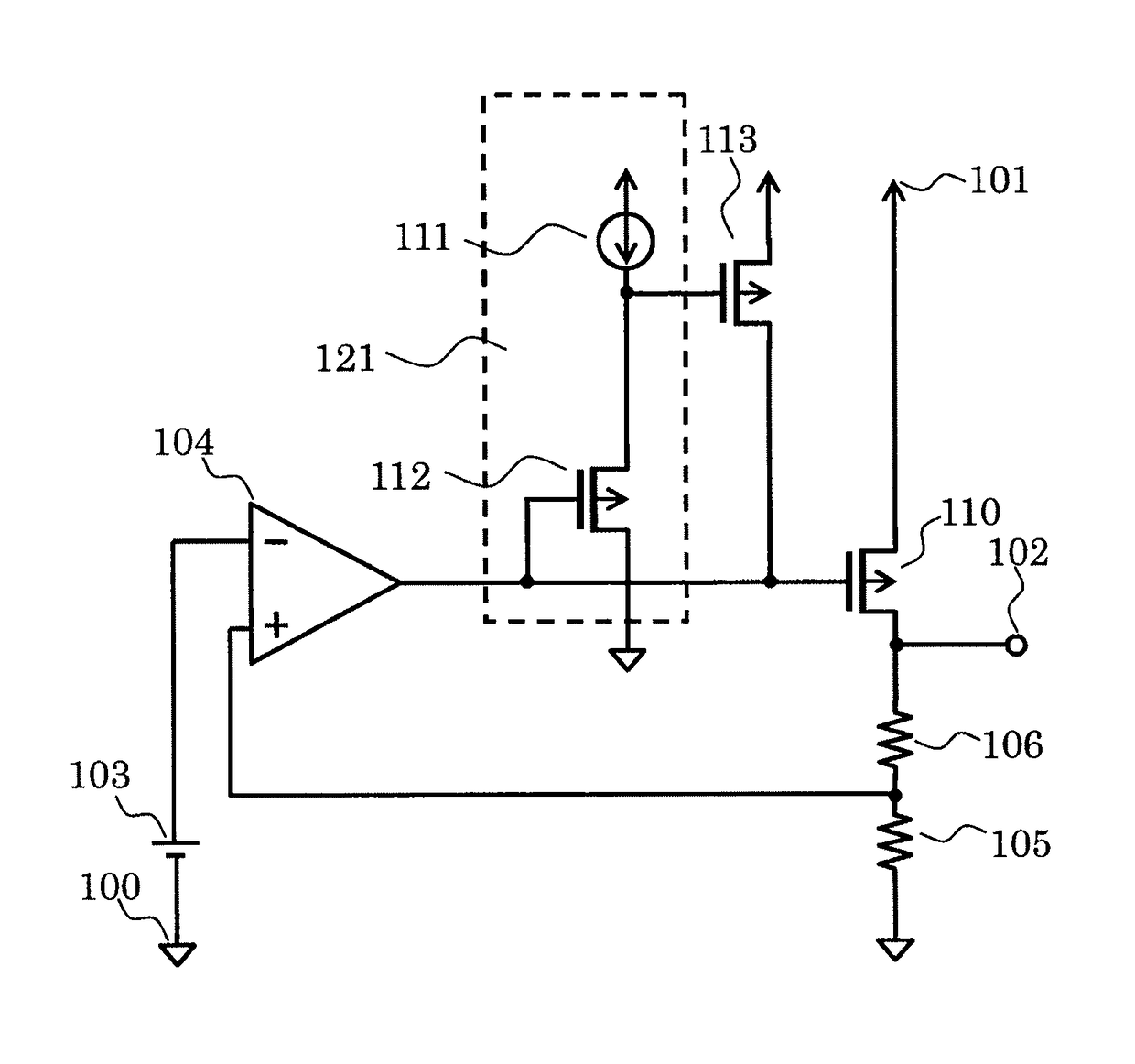
[0020]FIG. 1 is a circuit diagram of a voltage regulator according to a first embodiment of the present invention.
[0021]The voltage regulator according to the first embodiment includes an error amplifier circuit 104, a reference voltage circuit 103, an output transistor 110, PMOS transistors 112 and 113, resistors 105 and 106, a constant current circuit 111, a ground terminal 100, an output terminal 102, and a power supply terminal 101. The constant current circuit 111 and the PMOS transistor 112 form a level shift circuit 121. The PMOS transistor 113 is a clamp circuit for a gate of the output transistor 110.
[0022]Next, connections in the voltage regulator according to the first embodiment are described.
[0023]The resistor 105 and the resistor 106 are connected in series between the output terminal 102 and the ground terminal 100. The error amplifier circuit 104 has an inverting input terminal connected to a positive electrode of the reference voltage circuit 103 and a non-inverting...
second embodiment
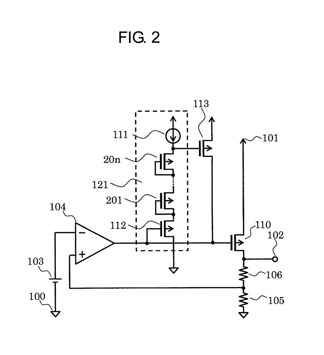
[0034]FIG. 2 is a circuit diagram of a voltage regulator according to a second embodiment of the present invention. FIG. 2 differs from FIG. 1 in that n PMOS transistors 201 to 20n that are diode-connected impedance elements are connected between the source of the PMOS transistor 112 and the gate of the PMOS transistor 113. The rest is the same as in FIG. 1.
[0035]An operation of the voltage regulator according to the second embodiment is described. A normal operation is the same as that in the first embodiment.
[0036]When a threshold value of the diode-connected PMOS transistor is represented by Vth similarly to the threshold value of the PMOS transistor 112, VLS=|Vth|+n×|Vth|=(n+1)×|Vth| holds, and Expression (3) is then expressed as follows.
VDRVG2)×|Vth| (5)
Based on Expression (5), the PMOS transistor 113 starts to cause a current to flow when the voltage VDRVG decreases from the power supply voltage VDD to be smaller than VDD−(n+2)×|Vth|, thereby starting the clamping operation.
[...
third embodiment
[0039]FIG. 3 is a circuit diagram of a voltage regulator according to a third embodiment of the present invention. FIG. 3 differs from FIG. 1 in that a resistor 301 that is an impedance element is connected between the source of the PMOS transistor 112 and the gate of the PMOS transistor 113. The rest is the same as in FIG. 1.
[0040]An operation of the voltage regulator according to the third embodiment is described. A normal operation is the same as that in the first embodiment.
[0041]When a resistance value of the resistor 301 is represented by R1 and a current of the constant current circuit 111 is represented by I1, Expression (3) is then expressed as follows.
VDRVG2×|Vth|−I1×R1 (6)
Based on Expression (6), the PMOS transistor 113 starts to cause a current to flow when the voltage VDRVG decreases from the power supply voltage VDD to be smaller than VDD−2×|Vth|−I1×R1, thereby starting the clamping operation.
[0042]With this configuration, the clamp level can be easily adjusted by cha...
PUM
 Abstract
Description
Claims
Application Information