Method for producing a circuit board and circuit board
What is AI technical title?
AI technical title is built by Patsnap AI team. It summarizes the technical point description of the patent document.
a technology of circuit board and circuit board, which is applied in the direction of printed circuit manufacturing, printed circuit aspects, lamination printed circuit boards, etc., can solve the problem of design with a relatively low level of thermal resistance between the inlays and the cooling body
Active Publication Date: 2017-12-19
VITESCO TECH GERMANY GMBH +1
View PDF11 Cites 0 Cited by
Summary
Abstract
Description
Claims
Application Information
AI Technical Summary
This helps you quickly interpret patents by identifying the three key elements:
Problems solved by technology
Method used
Benefits of technology
Benefits of technology
[0006]The procedure according to the invention allows inlays to be positioned in a printed-circuit-board layer with very small spacings apart from one another, since the positioning elements can be designed very precisely, even with small dimensions, in the punching operation. The small distances or gaps between the individual inlays mean that, during the following laminating operation with a prepreg layer positioned above, comparatively little liquefied resin material is required between the inlays, and this renders a layer construction with only a small number of thin prepregs possible, which results in a design with a relatively low level of thermal resistance between the inlays and a cooling body connected to one of the surfaces. According to the invention, it is thus possible to realize gaps between the inlays in the order of magnitude of around 100 μm (in relation to prior-art gap widths ranging from 1 to 2 mm).
Problems solved by technology
The small distances or gaps between the individual inlays mean that, during the following laminating operation with a prepreg layer positioned above, comparatively little liquefied resin material is required between the inlays, and this renders a layer construction with only a small number of thin prepregs possible, which results in a design with a relatively low level of thermal resistance between the inlays and a cooling body connected to one of the surfaces.
Method used
Image
Click on the blue label to locate the original text in one second.
Reading with bidirectional positioning of images and text.
Examples
Embodiment Construction
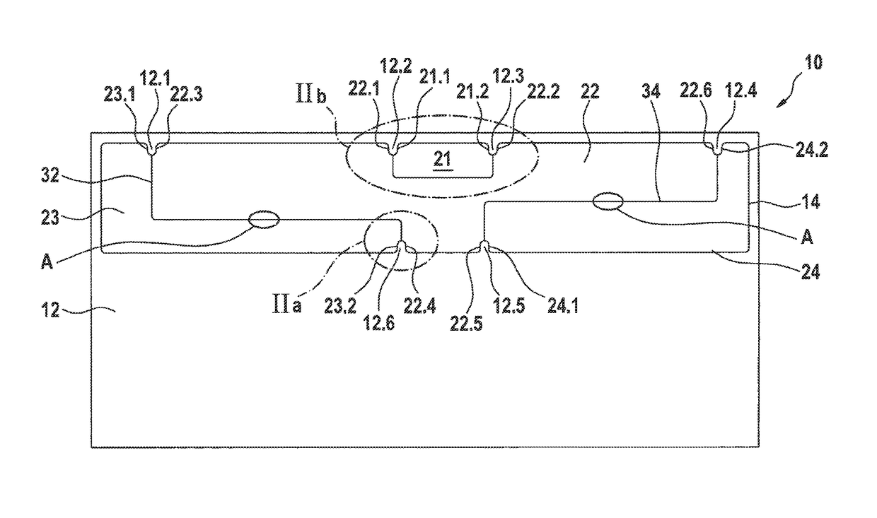
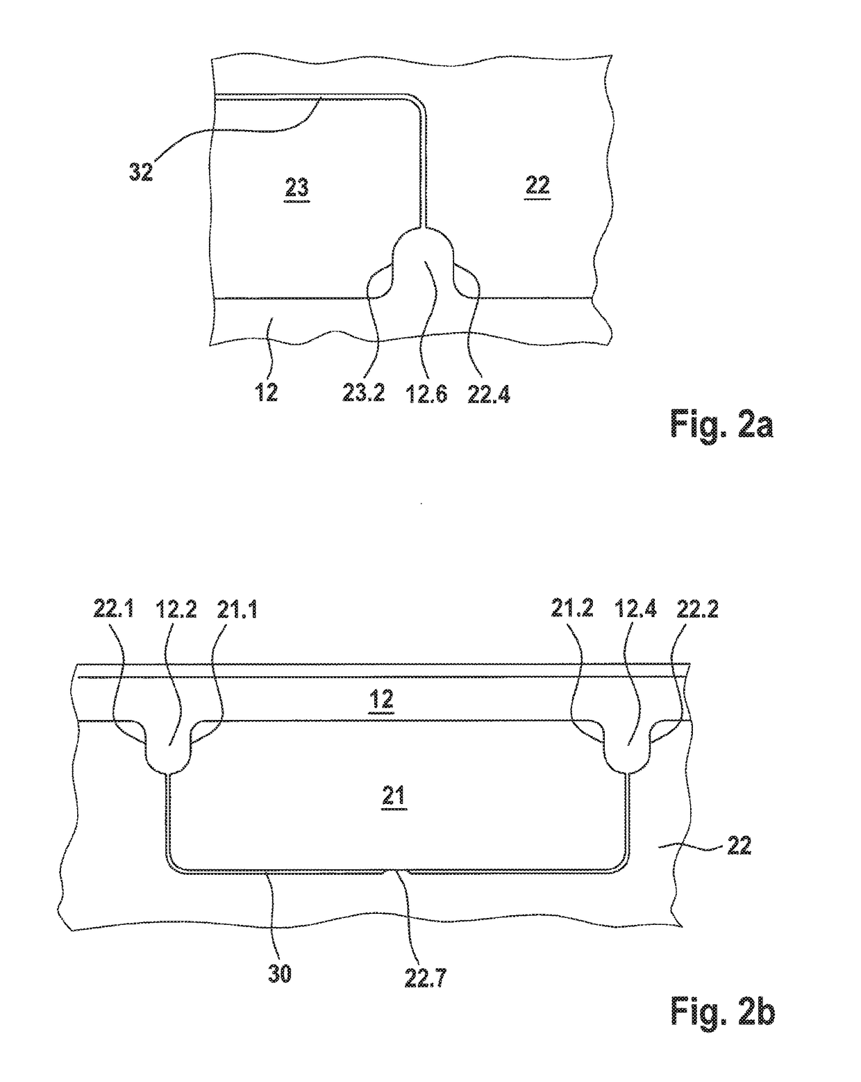
[0019]In the figures, like reference signs denote like or similar elements.
[0020]FIG. 1 shows a plan view of a layer sequence for producing a printed circuit board 10 during the production process.
[0021]The uppermost layer, which is directed toward the person viewing FIG. 1, is a printed-circuit-board layer 12 made of a non-conductive printed-circuit-board material, for example FR4 or the like.
[0022]The term “positioning element” is used, within the context of the present patent application and of the description which follows, to denote any kind of element which is formed on an inlay, in particular an inlay edge, and is suitable for positioning the inlay when it is inserted into a recess provided for it in a printed-circuit-board layer. Such positioning elements may be in particular, but not exclusively, lugs and / or convexities and / or protrusions and / or cutouts and / or indents and / or set-back portions or the like. The positioning elements may be provided on one or more inlay edges o...
PUM
Abstract
A method of producing a printed circuit board (10) with a plurality of inlays (21, 22, 23, 24), having the following steps: supplying a plurality of inlays (21, 22, 23, 24), of which at least one inlay has at least one positioning element (21.1, 21.2; 22.1 to 22.7; 23.1, 23.2; 24.1, 24.2); building up a layer sequence from a plurality of printed-circuit-board layers, with at least one recess (14) for accommodating inlays, wherein, prior to the step of the plurality of inlays (21, 22, 23, 24) being inserted, the recess (14) is defined in an uppermost layer (12) by a frame made of non-conductive printed-circuit-board material; inserting the plurality of inlays (21, 22, 23, 24) into the recess (14) defined by the frame; covering the inlays (21, 22, 23, 24) with a non-conductive printed-circuit-board material; laminating the layer sequence, and removing at least the positioning elements (21.1, 21.2; 22.1 to 22.7; 23.1, 23.2; 24.1, 24.2) which establish a conductive contact between neighboring inlays.
Description
TECHNICAL FIELD[0001]The present invention relates to the field of printed-circuit-board production and, in particular, to the production of inlays for insertion into printed circuit boards or into printed circuit boards which have the insertion of inlays included in their production process.DESCRIPTION OF THE PRIOR ART[0002]Inlays for printed circuit boards are known and widely used. An example to mention would be the multi-layered printed circuit board which is known from DE 10 2005 047 025 A1 and comprises an inlay which is made of a solid copper block and is inserted into a recess provided for it in the printed-circuit-board layer sequence.[0003]Such inlays are usually produced individually, in particular by virtue of being punched out of a copper plate, or a plate made of some other suitable material, in order then to be inserted individually into recesses provided for them in a printed circuit board (or in a printed circuit board in an interim production step).[0004]In contras...
Claims
Application Information
Patent Timeline
Application Date:The date an application was filed.
Publication Date:The date a patent or application was officially published.
First Publication Date:The earliest publication date of a patent with the same application number.
Issue Date:Publication date of the patent grant document.
PCT Entry Date:The Entry date of PCT National Phase.
Estimated Expiry Date:The statutory expiry date of a patent right according to the Patent Law, and it is the longest term of protection that the patent right can achieve without the termination of the patent right due to other reasons(Term extension factor has been taken into account ).
Invalid Date:Actual expiry date is based on effective date or publication date of legal transaction data of invalid patent.

