Detection devices and methods
a detection device and detector technology, applied in the direction of radiation intensity measurement, measurement with semiconductor devices, radiation controlled devices, etc., can solve the problems of long-standing shortage of sup>3/sup>he, risk of nuclear proliferation, and urgent replacement, etc., and achieve the effect of small size and reliabl
- Summary
- Abstract
- Description
- Claims
- Application Information
AI Technical Summary
Benefits of technology
Problems solved by technology
Method used
Image
Examples
example 1
[0069]An array included eight detectors. The detectors included silicon semiconductors and were placed on individually adjustable detector mounts and arranged to obtain annular views of the sample with the same solid angle. The detectors had the following specifications:
[0070]
ModelULTRA ion implanted(model: U016-300-100)Contact500ÄActive Area300mm2Minimum Depletion Depth100μmResolution (FWHM)16keV @ 5.486 MeV alpha
[0071]The detectors and eight preamplifiers were placed in a stainless steel right circular cylinder (61 cm×61 cm in size) and a vacuum of 10−6 Torr was maintained during the experiments.
[0072]A thermal neutron beam (10 mm in diameter) provided neutrons at a 500 kW thermal, light water, and pool-type reactor. The reactor operated at 5 kW for this measurement and delivered a thermal equivalent neutron flux of about 8.6×104 cm−2-s−1 and a gamma dose rate of about 25 mR h−1.
[0073]A thin Gd foil (1.25 cm×1.25 cm×0.0025 cm) was mounted on the sample holder inside the vacuum cha...
example 2
[0078]Monte Carlo simulations were conducted using Monte Carlo N-Particle Transport Code (MCNP5) and Software for Optimization of Radiation Detectors (SWORD) in order to observe the internal conversion electron energy spectrum following thermal neutron absorption in Gd. A beam of 0.0253 eV thermal neutrons was perpendicularly incident on a 10 μm thick natural Gd foil and a 200 μm thick silicon detector was used to tally the energy deposition of the Gd(n,γ)Gd* reaction products. An internal conversion electron source was created in the Gd foil for MCNP5 simulation.
[0079]A comparison of the spectra obtained by MCNP5 and SWORD revealed a close resemblance between these simulations and similarity to the results of Example 1.
example 3
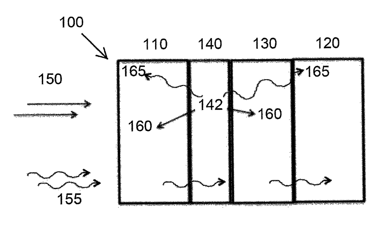
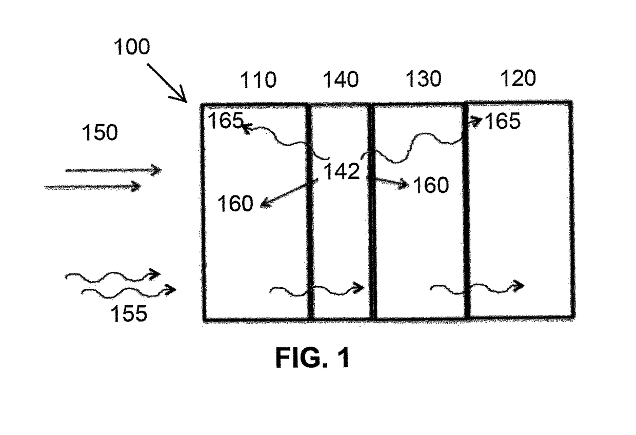
[0080]A SWORD simulation was carried out using the setup illustrated in FIG. 1. The Gd-containing layer was a 10 μm thick foil. The separator was a 100 μm thick polyethylene separator. The detectors were both 200 μm thick Si detectors.
[0081]The internal conversion electron results resembled both the experimental results of Example 1 and the simulation results of Example 2 despite a slightly different geometry.
PUM
 Abstract
Description
Claims
Application Information


