
Eureka
For R&D, Eureka makes reading and utilizing patents & technical documents easy.
Eureka AIR
Designed for self-driven R&D workflows. Generate viable solutions, solve complex R&D challenges, empower your innovation with AI.

Eureka Materials
Designed for material experts only. Revolutionize your material R&D, from search, analyze, to developing new materials.

TechResearch
Generate reliable direction feasibility study reports for your R&D in just a few steps.

TechSeek
Discover and master advanced knowledge NOW. Basics, ideas, possibilities, all at once.

TechMind
As an expert in R&D Theories, TechMind can generates customized viable solutions instantly.

TechRisk
Analyze your overall solution with one click, know your potential R&D risks in advance.

TechMonitor
Get weekly tech updates, stay abreast of the latest tech innovations and key insights.
Semiconductor device
- Summary
- Abstract
- Description
- Claims
- Application Information
AI Technical Summary
Benefits of technology
Problems solved by technology
Method used
Image

Examples
first embodiment
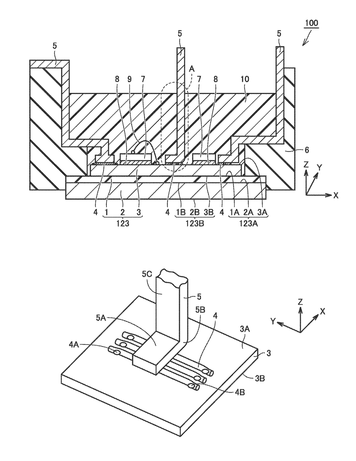
[0028]The configuration of a semiconductor device of the present embodiment will be hereinafter described with reference to FIGS. 1 to 5. In addition, the X direction, the Y direction and the Z direction are introduced for the sake of explanation.
[0029]Referring to FIG. 1, a semiconductor device 100 of the present embodiment mainly includes an insulating substrate 1, a base plate 2, a circuit pattern 3, a wire 4, an electrode terminal 5, a case 6, and a semiconductor element 7.
[0030]Insulating substrate 1 is formed of an insulating material such as commonly-known ceramics or resin, and is provided as a flat plate-shaped member, for example, having a rectangular shape in a plan view. Insulating substrate 1 has one main surface 1A on the upper side in FIG. 1 and the other main surface 1B on the opposite side of this one main surface 1A, that is, on the lower side in FIG. 1. Base plate 2 is formed in a rectangular flat plate shape and joined to the other main surface 1B of insulating s...
second embodiment
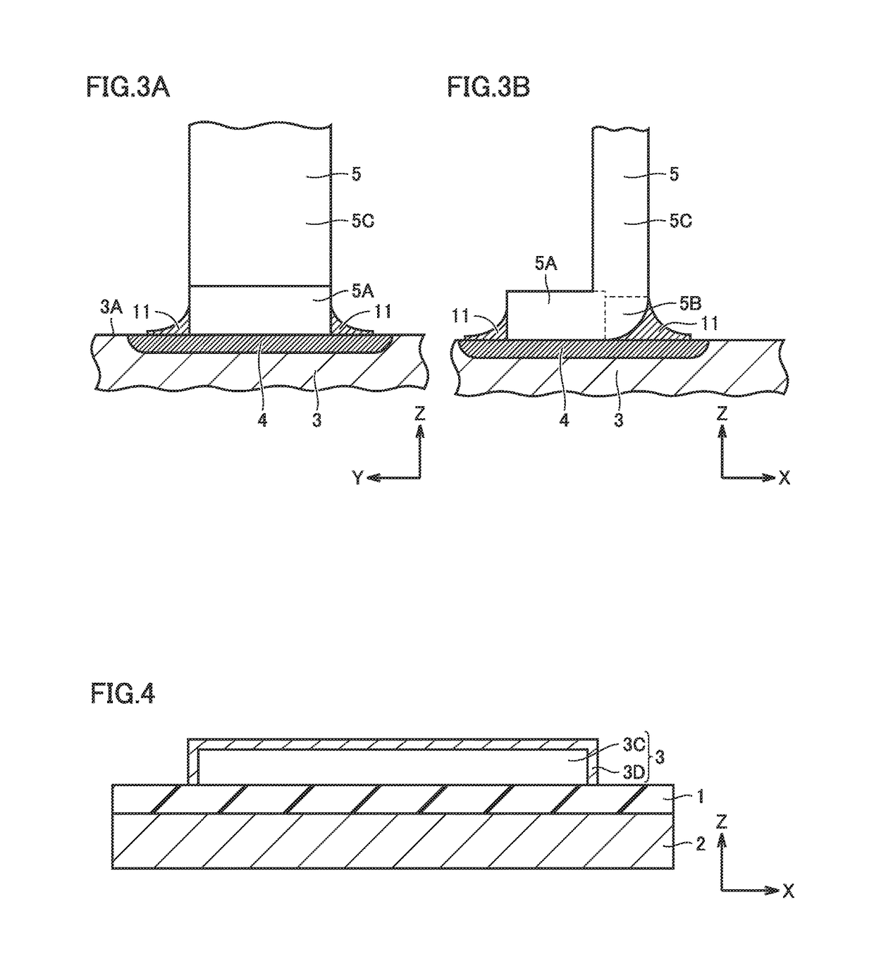
[0069]Referring to FIG. 10, also in the semiconductor device of the present embodiment, electrode terminal 5, wire 4 and circuit pattern 3 are joined to each other using ultrasonic joining machine 12, as in the semiconductor device of the first embodiment. Also in the semiconductor device of the present embodiment, all of the plurality of wires 4 extend in the Y direction, for example, so as to be spaced apart from each other in the X direction. However, when comparing FIG. 10 with FIG. 6, in the present embodiment, at least one of the plurality of wires 4 is arranged so as to extend in the region overlapping bent portion 5B in a plan view. In this point, the present embodiment is different from the first embodiment in which all of the plurality of wires 4 are arranged so as to extend in the region overlapping horizontally extending portion 5A in a plan view. Also in the present embodiment, as shown in FIG. 10, for example, one of the plurality of wires 4 extends in the region overl...
third embodiment
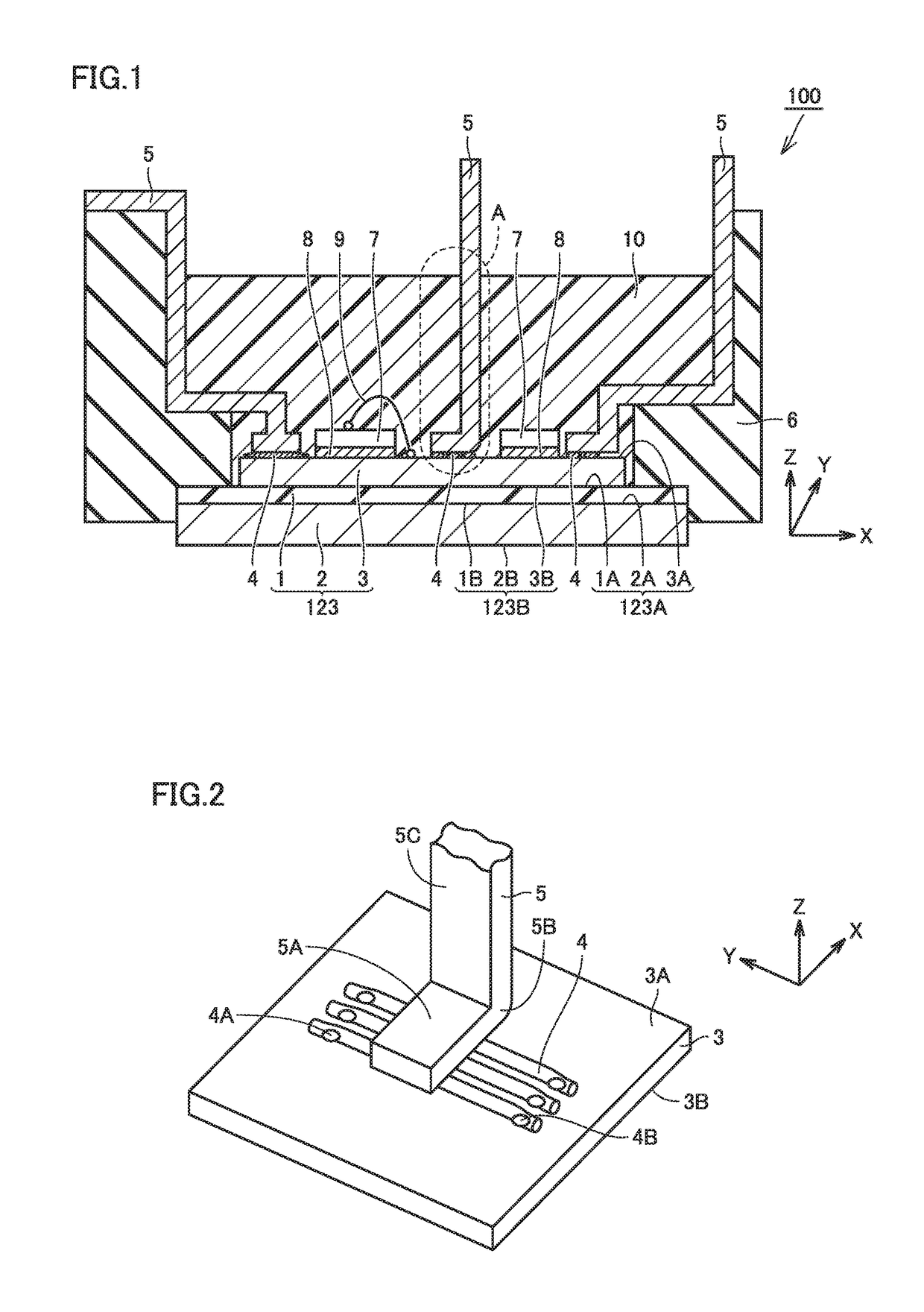
[0080]Referring to FIG. 13, in the semiconductor device of the present embodiment, wire 4 extends in a direction different from that in the case of semiconductor device 100 of the first embodiment. Specifically, when comparing FIG. 13 with FIG. 2, in the present embodiment, wire 4 joined onto one main surface 3A of circuit pattern 3 extends in the X direction, that is, in the direction connecting horizontally extending portion 5A and bent portion 5B. In this point, the present third embodiment is different from the first embodiment shown in FIG. 2 in which wire 4 extends in the Y direction, that is, in the direction crossing the direction connecting horizontally extending portion 5A and bent portion 5B.
[0081]The semiconductor device of the present embodiment is different from that of the first embodiment only in the above-described point, but is identical in other points to that of the first embodiment. Accordingly, the same components are designated by the same reference characters...
PUM
 Abstract
Description
Claims
Application Information
 - R&D Engineer
- R&D Manager
- IP Professional
- Industry Leading Data Capabilities
- Powerful AI technology
- Patent DNA Extraction
Browse by: Latest US Patents, China's latest patents, Technical Efficacy Thesaurus, Application Domain, Technology Topic, Popular Technical Reports.
© 2024 PatSnap. All rights reserved.Legal|Privacy policy|Modern Slavery Act Transparency Statement|Sitemap|About US| Contact US: help@patsnap.com