Photomask blank
a technology of photoresist and blank, which is applied in the field of photoresist blank, can solve the problems of difficult to accurately transfer the resist pattern to the chromium-containing film, deformation of the resist pattern, damage to the resist film, etc., and achieve the effect of reducing the thickness of the photoresist film, reducing the load on the photoresist, and high etching ra
- Summary
- Abstract
- Description
- Claims
- Application Information
AI Technical Summary
Benefits of technology
Problems solved by technology
Method used
Image
Examples
example 1
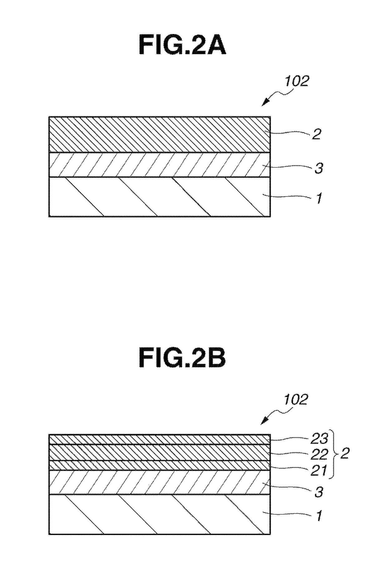
[0099]DC magnetron sputtering deposition was carried out on a quartz substrate of 152 mm squares and 6 mm thick. By sputtering a silicon target and feeding 15 sccm (flow rate) of Ar gas and 30 sccm of N2 gas as the sputtering gas into the sputtering chamber, a SiN film of 62 nm thick was deposited on the substrate as a halftone phase shift film.
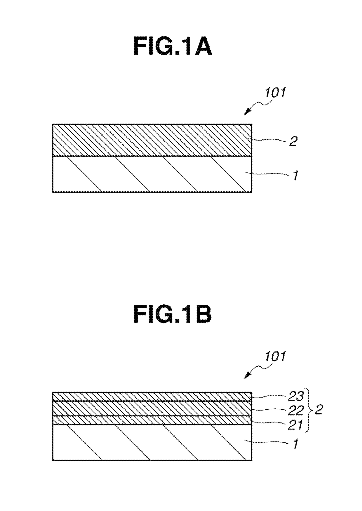
[0100]DC magnetron sputtering deposition was carried out by sputtering a metallic chromium target and feeding 45 sccm of N2 gas as the sputtering gas into the sputtering chamber. A CrN layer of 45 nm thick was formed on the halftone phase shift film. There was obtained a photomask blank having a chromium-containing film of monolayer structure as a light-shielding film. The chromium-containing film had an optical density of 2.1 with respect to ArF excimer layer (wavelength 193 nm), and the sum of optical densities of chromium-containing film and halftone phase shift film was 3.0.
example 2
[0101]DC magnetron sputtering deposition was carried out on a quartz substrate of 152 mm squares and 6 mm thick. By sputtering a silicon target and feeding 15 sccm (flow rate) of Ar gas and 30 sccm of N2 gas as the sputtering gas into the sputtering chamber, a SiN film of 62 nm thick was deposited on the substrate as a halftone phase shift film.
[0102]DC magnetron sputtering deposition was carried out by sputtering a metallic chromium target and feeding 45 sccm of N2 gas and 2 sccm of O2 gas as the sputtering gas into the sputtering chamber. A CrON layer of 46 nm thick was formed on the halftone phase shift film. There was obtained a photomask blank having a chromium-containing film of monolayer structure as a light-shielding film. The chromium-containing film had an optical density of 2.1 with respect to ArF excimer layer (wavelength 193 nm), and the sum of optical densities of chromium-containing film and halftone phase shift film was 3.0.
example 3
[0103]DC magnetron sputtering deposition was carried out on a quartz substrate of 152 mm squares and 6 mm thick. By sputtering a silicon target and feeding 15 sccm (flow rate) of Ar gas and 30 sccm of N2 gas as the sputtering gas into the sputtering chamber, a SiN film of 62 nm thick was deposited on the substrate as a halftone phase shift film.
[0104]DC magnetron sputtering deposition was carried out by sputtering a metallic chromium target and feeding 45 sccm of N2 gas as the sputtering gas into the sputtering chamber. A CrN layer of 44 nm thick mainly functioning as a conductive layer was formed on the halftone phase shift film. Next, DC magnetron sputtering deposition was carried out by sputtering a metallic chromium target and feeding 10 sccm of Ar gas, 30 sccm of N2 gas, and 15 sccm of O2 gas as the sputtering gas into the sputtering chamber. A CrON layer of 1 nm thick mainly functioning as an antireflective layer on the side remote from the substrate was formed. In this way, t...
PUM
| Property | Measurement | Unit |
|---|---|---|
| optical density | aaaaa | aaaaa |
| optical density | aaaaa | aaaaa |
| aspect ratio | aaaaa | aaaaa |
Abstract
Description
Claims
Application Information


