Matrix of sensor units each comprising a first sensing element and a second sensing element
a sensor unit and matrix technology, applied in the field of sensors, can solve problems such as accidental application of force, and achieve the effect of high convenient or reliable, highly convenient or reliabl
- Summary
- Abstract
- Description
- Claims
- Application Information
AI Technical Summary
Benefits of technology
Problems solved by technology
Method used
Image

Examples
embodiment 1
(Embodiment 1)
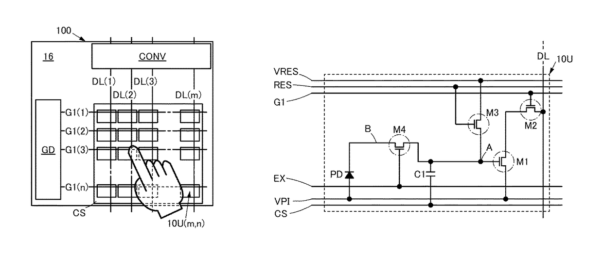
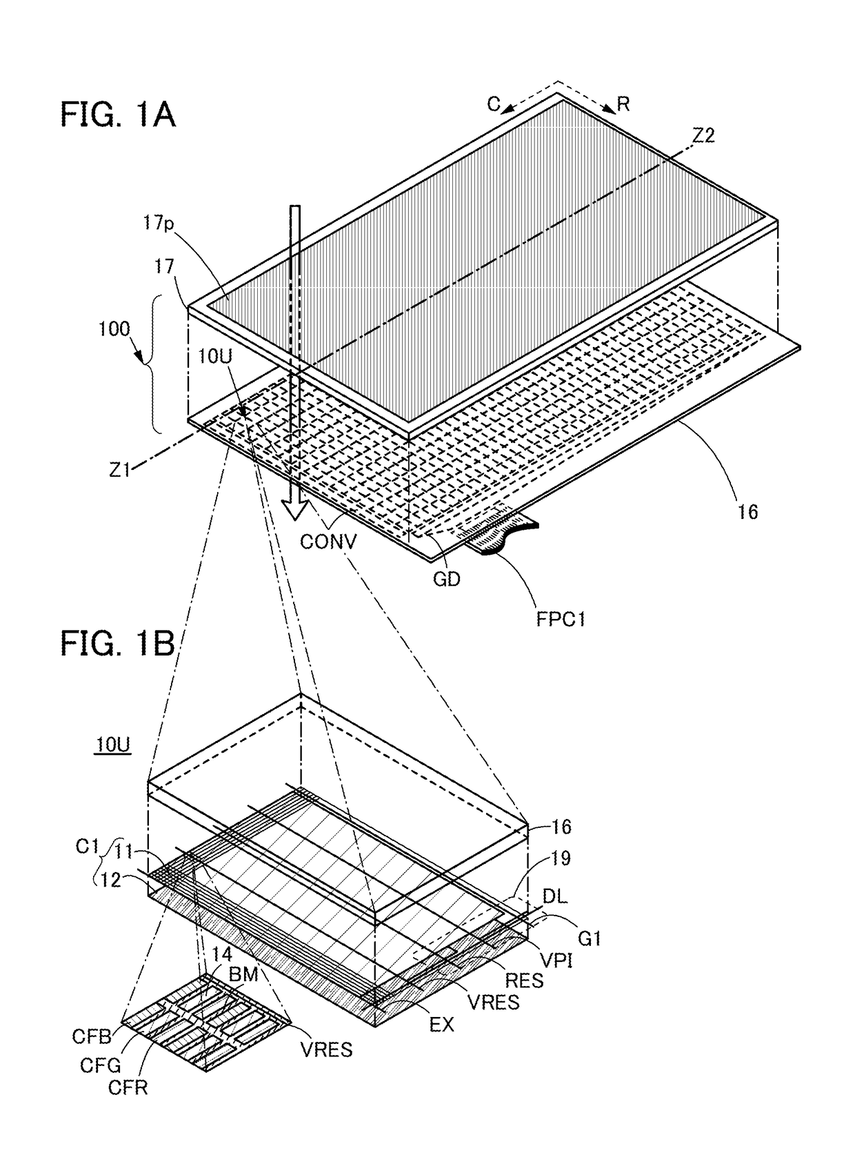
[0071]In this embodiment, a structure of an input device of one embodiment of the present invention is described with reference to FIGS. 1A and 1B and FIG. 2.
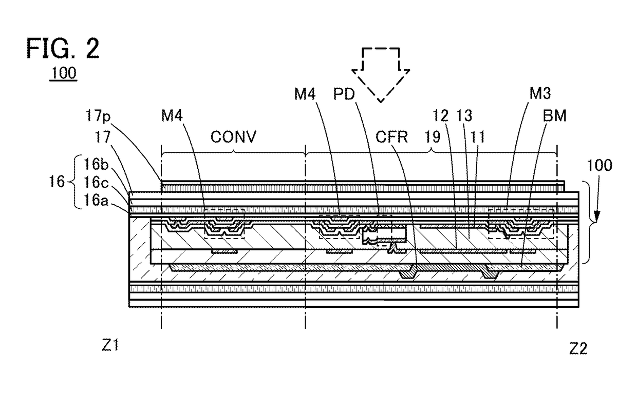
[0072]FIGS. 1A and 1B illustrate a structure of an input device 100 of one embodiment of the present invention. FIG. 2 is a cross-sectional view illustrating a structure of the input device 100 of one embodiment of the present invention.
[0073]FIG. 1A is a projection view of the input device 100 of one embodiment of the present invention. FIG. 1B is an enlarged projection view of a sensor unit 10U, which is part of FIG. 1A.
[0074]FIG. 2 is a cross-sectional view illustrating a cross-sectional structure of the input device 100 of one embodiment of the present invention along the line Z1-Z2 in FIG. 1A.
[0075]The input device 100 described in this embodiment includes a plurality of sensor units 10U arranged in a matrix, scan lines G1 which are placed along the row direction (indicated by the arrow R in the figure) and t...
embodiment 2
(Embodiment 2)
[0160]In this embodiment, a structure of an input device of one embodiment of the present invention is described with reference to FIGS. 3A to 3D2.
[0161]FIGS. 3A to 3D2 illustrate a structure of the input device 100 of one embodiment of the present invention.
[0162]FIG. 3A is a block diagram illustrating a configuration of the input device 100 of one embodiment of the present invention. FIG. 3B is a circuit diagram illustrating a configuration of the converter CONV which can be used in the input device 100 in FIG. 3A. FIG. 3C is a circuit diagram illustrating a configuration of the sensing circuit 19 which can be used in the input device 100 in FIG. 3A.
[0163]FIGS. 3D1 and 3D2 are timing charts each illustrating a driving method of the sensor unit 10U which can be used in the input device 100 of one embodiment of the present invention.
[0164]The input device 100 described in this embodiment includes a plurality of sensor units 10U arranged in a matrix, the scan lines G1 w...
embodiment 3
(Embodiment 3)
[0218]In this embodiment, a structure of an input device of one embodiment of the present invention is described with reference to FIGS. 4A to 4D2.
[0219]FIGS. 4A to 4D2 illustrate a structure of the input device 100B of one embodiment of the present invention.
[0220]FIG. 4A is a block diagram illustrating a configuration of the input device 100B of one embodiment of the present invention. FIG. 4B is a circuit diagram illustrating a configuration of the converter CONV which can be used in the input device 100B in FIG. 3A. FIG. 4C is a circuit diagram illustrating a configuration of the sensing circuit 19B which can be used in the input device 100B in FIG. 4A.
[0221]FIGS. 4D1 and 4D2 are timing charts each illustrating a driving method of the sensor units 10UB which can be used in the input device 100B of one embodiment of the present invention.
[0222]The input device 100B described in this embodiment includes a plurality of sensor units 10UB arranged in a matrix, the scan ...
PUM
 Abstract
Description
Claims
Application Information
 - R&D
- Intellectual Property
- Life Sciences
- Materials
- Tech Scout
- Unparalleled Data Quality
- Higher Quality Content
- 60% Fewer Hallucinations
Browse by: Latest US Patents, China's latest patents, Technical Efficacy Thesaurus, Application Domain, Technology Topic, Popular Technical Reports.
© 2025 PatSnap. All rights reserved.Legal|Privacy policy|Modern Slavery Act Transparency Statement|Sitemap|About US| Contact US: help@patsnap.com