
Separate read and write address decoding in a memory system to support simultaneous memory read and write operations

a memory system and address decoding technology, applied in the field of memory systems, can solve the problem that multiple memory bit cell rows cannot be selected in the memory array in response to a memory write operation, and achieve the effect of avoiding circuit conflicts, minimizing power, performance and area (ppa) of the memory system

Active Publication Date: 2018-01-16
QUALCOMM INC
View PDF22 Cites 5 Cited by
  • Summary
  • Abstract
  • Description
  • Claims
  • Application Information

AI Technical Summary

Benefits of technology

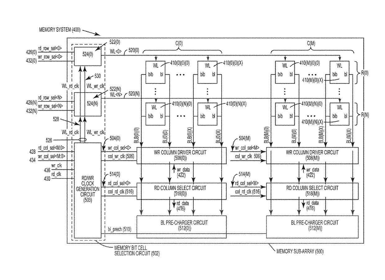
This patent relates to a memory system that supports simultaneous memory read and write operations. By separating read and write address decoding, the system can avoid circuit conflicts and use single port memory bit cells to minimize power, performance, and area. The memory array may be segregated into smaller sub-arrays to increase memory read operation success. The system can also allow for simultaneous memory read and write operations to different memory addresses in different sub-arrays without prioritizing a write row select over a read row select. This separation of read and write address decoding may further reduce complexity in routing and power consumption.

Problems solved by technology

However, multiple memory bit cell rows cannot be selected in the memory array in response to a memory write operation, because the write data will be written to multiple memory bit cells rows (i.e., more than one memory address location) in an undesired manner.

Method used


Image

  • Separate read and write address decoding in a memory system to support simultaneous memory read and write operations
  • Separate read and write address decoding in a memory system to support simultaneous memory read and write operations
  • Separate read and write address decoding in a memory system to support simultaneous memory read and write operations

Examples


Embodiment Construction

[0025]With reference now to the drawing figures, several exemplary aspects of the present disclosure are described. The word “exemplary” is used herein to mean “serving as an example, instance, or illustration.” Any aspect described herein as “exemplary” is not necessarily to be construed as preferred or advantageous over other aspects.

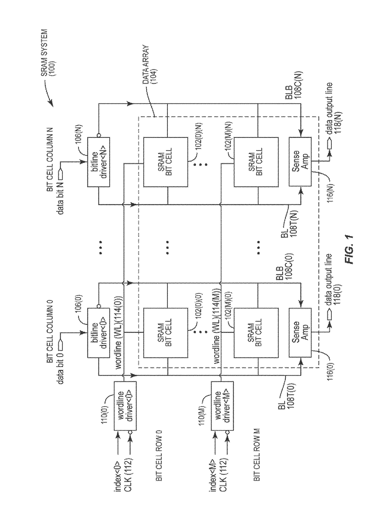
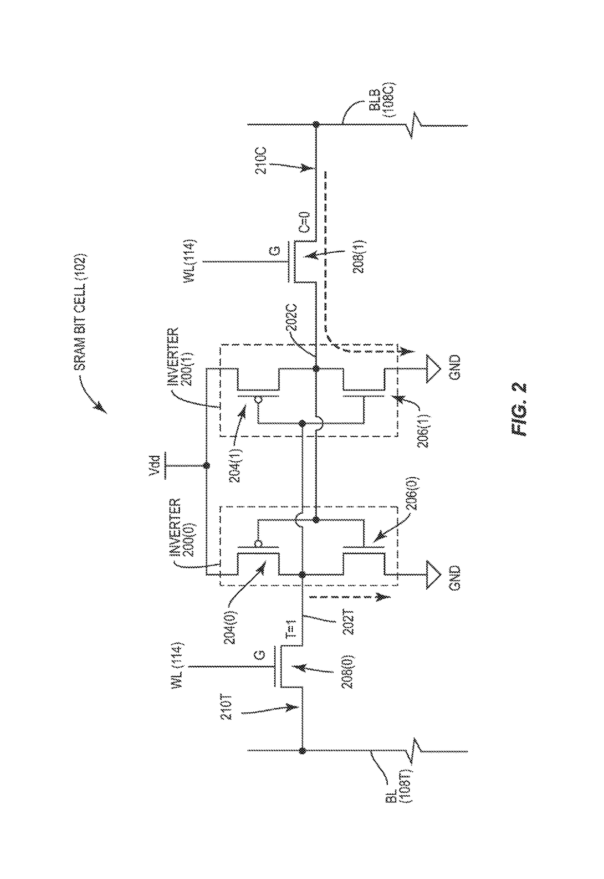
[0026]Aspects of the present disclosure involve separate read and write address decoding in a memory system to support simultaneous memory read and write operations. By separating read and write address decoding, a memory system can avoid circuit conflicts even if employing single port memory bit cells that only include one port for conducting memory read and write operations. It may be desired to employ single port memory bit cells in the memory system as a non-limiting example to minimize power, performance, and area (PPA) of the memory system.

[0027]In this regard, in exemplary aspects disclosed herein, a memory system includes a memory array compri...


PUM


Abstract

Memory systems that provide separate read and write address decoding to support simultaneous memory read and write operations are disclosed. Separating read and write address decoding can avoid circuit conflicts for a simultaneous memory read and write operation even if employing single port memory bit cells. The read and write addresses of respective read and write operations are separately decoded into read and write row and column selects driven to a memory array so that simultaneous read and write operations are not affected by each other. To avoid a circuit conflict for a simultaneous read and write operation, the memory system is configured to prioritize a write row select over a read row select to drive a row of memory bit cells in the memory array. In this manner, that write operation will always be successful regardless of whether the read and write row select are to the same row.

Description

PRIORITY APPLICATION[0001]The present application claims priority under 35 U.S.C. §119(e) to U.S. Provisional Patent Application Ser. No. 62 / 403,740 filed on Oct. 4, 2016, and entitled “SEPARATE READ AND WRITE ADDRESS DECODING IN A MEMORY SYSTEM TO SUPPORT SIMULTANEOUS MEMORY READ AND WRITE OPERATIONS,” the contents of which is incorporated herein by reference in its entirety.BACKGROUNDI. Field of the Disclosure[0002]The technology of the disclosure relates generally to memory systems for processor-based systems, and more particularly to memory systems, such as static random access memory (SRAM) systems employing SRAM bit cells, capable of performing simultaneous memory read and write operations.II. Background[0003]Processor-based computer systems include memory for data storage. Different types of memory exist, each possessing certain unique features. For example, static random access memory (SRAM) is a type of memory that can be employed in processor-based computer systems. SRAM c...

Claims


Application Information

Patent Timeline
IPC IPC(8): G11C8/10G11C11/419G11C11/418
CPCG11C11/419G11C11/418G11C7/1015G11C8/08G11C8/10G11C2207/2209
Inventor GARG, MANISH
Owner QUALCOMM INC
Learn More