

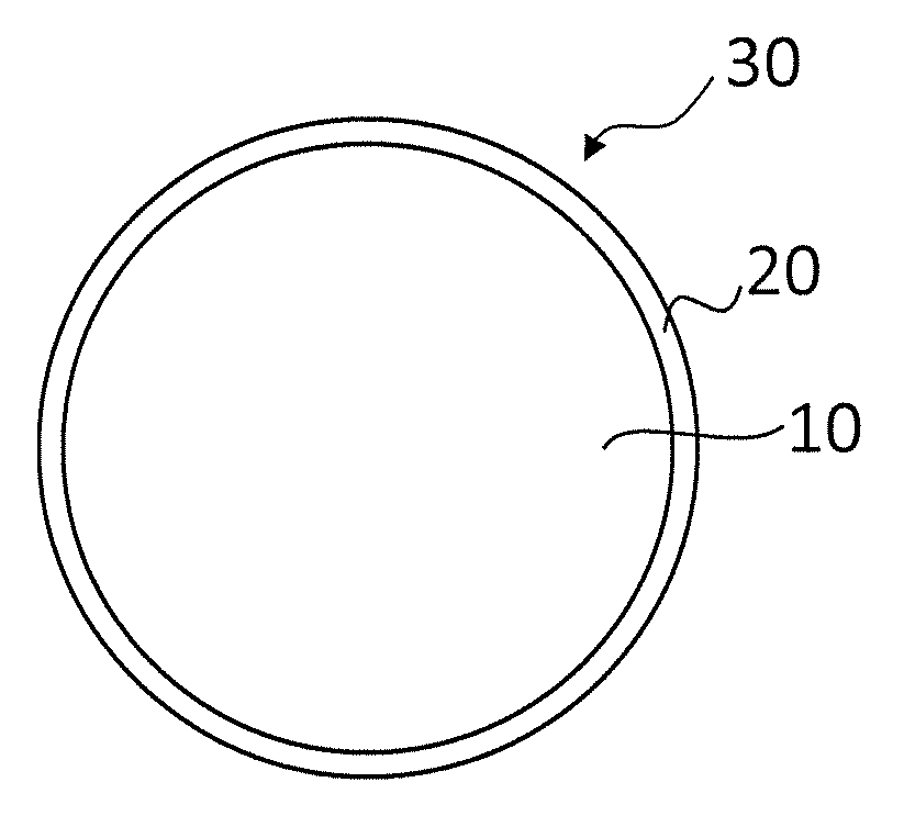
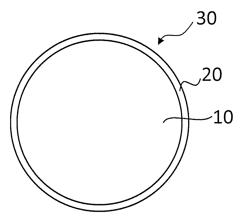
Bonding wire for semiconductor device
a technology for bonding wires and semiconductor devices, applied in the direction of layered products, basic electric elements, chemistry apparatuses and processes, etc., can solve the problems of inferior bonding reliability, ball formability, and poor bonding reliability so as to improve the bonding reliability and improve the longevity of ball bonded parts
- Summary
- Abstract
- Description
- Claims
- Application Information
AI Technical Summary
Benefits of technology
Problems solved by technology
Method used
Image

Examples
examples
[0060]The following specifically describes the bonding wire according to an embodiment of the present invention with reference to examples.
[0061](Sample)
[0062]First, the following describes a method for manufacturing a sample. Cu as a raw material of the core material with a purity of 99.99% by mass or more and containing inevitable impurities as the remainder was used. Ga, Ge, Ni, Ir, Pt, Pd, B, P, and Mg with a purity of 99% by mass or more and containing inevitable impurities as the remainder were used. Ga, Ge, Ni, Ir, Pt, Pd, B, P, and Mg as additive elements to the core material are mixed so that the wire or the core material will have a target composition. Regarding the addition of Ga, Ge, Ni, Ir, Pt, Pd, B, P, and Mg, although they can be mixed singly, or alternatively, they may be mixed so as to be a desired amount using a Cu master alloy containing the additive elements manufactured in advance if the element has a high melting point as a single body or if the element is add...
PUM
| Property | Measurement | Unit |
|---|---|---|
| thickness | aaaaa | aaaaa |
| thickness | aaaaa | aaaaa |
| thickness | aaaaa | aaaaa |
Abstract
Description
Claims
Application Information