Display device and electronic device

a display device and electronic technology, applied in the direction of semiconductor devices, instruments, optics, etc., can solve the problems of affecting the characteristics of semiconductors, alignment defects are likely to be caused along the way, so as to reduce the number of alignment defects, increase the charge capacity, and increase the aperture ratio

Inactive Publication Date: 2018-03-13
SEMICON ENERGY LAB CO LTD
View PDF203 Cites 2 Cited by
  • Summary
  • Abstract
  • Description
  • Claims
  • Application Information

AI Technical Summary

Benefits of technology

[0009]In a liquid crystal display, when unevenness such as a step difference around a pixel is large, alignment defects are likely to be caused. The alignment defects are likely to be caused along, for example, a scan line and a data line that are connected to a transistor and a side of a step difference near a pixel electrode. Thus, part of an opening of a pixel that can be used as a display region needs to be covered with a light-blocking film (what is called a black matrix, and also referred to as BM). Accordingly, an aperture ratio of the pixel is lowered, and the display quality of an image is lowered.
[0013]As the capacitance value of a capacitor is increased, a period in which the alignment of liquid crystal molecules of a liquid crystal element can be kept constant in the state where an electric field is applied can be made longer. When the period can be made longer in a display device that displays a still image, the number of times of rewriting image data can be reduced, leading to a reduction in power consumption.
[0016]In view of the above problem, one object of one embodiment of the present invention is to provide a display device having fewer alignment defects. Further, another object of one embodiment of the present invention is to provide a display device having a high aperture ratio and including a capacitor which has increased charge capacity. Furthermore, another object of one embodiment of the present invention is to provide a display device having a high aperture ratio, including a capacitor with large charge capacity, and having fewer alignment defects.
[0018]Since the pixel electrode extends so as to intersect with the scan line, for example, an approximate half of a pixel can be positioned in a region divided by the scan lines and the data lines, and the other approximate half of the pixel can be positioned in an adjacent region divided by the scan lines and the data lines. With such an arrangement, an end portion of the pixel electrode is positioned away from the scan line; thus, a liquid crystal layer is not or is hardly affected by a step difference due to the scan line. Thus, the alignment defects of the liquid crystal layer due to the scan line can be reduced.
[0020]According to one embodiment of the present invention, a display device having fewer alignment defects can be provided. Further, a display device having a high aperture ratio and including a capacitor which has increased charge capacity can be provided. Furthermore, a display device having a high aperture ratio, including a capacitor with large charge capacity, and having fewer alignment defects can be provided.

Problems solved by technology

In a liquid crystal display, when unevenness such as a step difference around a pixel is large, alignment defects are likely to be caused.
The alignment defects are likely to be caused along, for example, a scan line and a data line that are connected to a transistor and a side of a step difference near a pixel electrode.
However, in the case where an oxide semiconductor is used as a semiconductor material included in the transistor, when impurities (typically, moisture or the like) contained in an organic resin enters the oxide semiconductor, which adversely affects the semiconductor characteristics.

Method used


Image

  • Display device and electronic device
  • Display device and electronic device
  • Display device and electronic device

Examples


embodiment 1

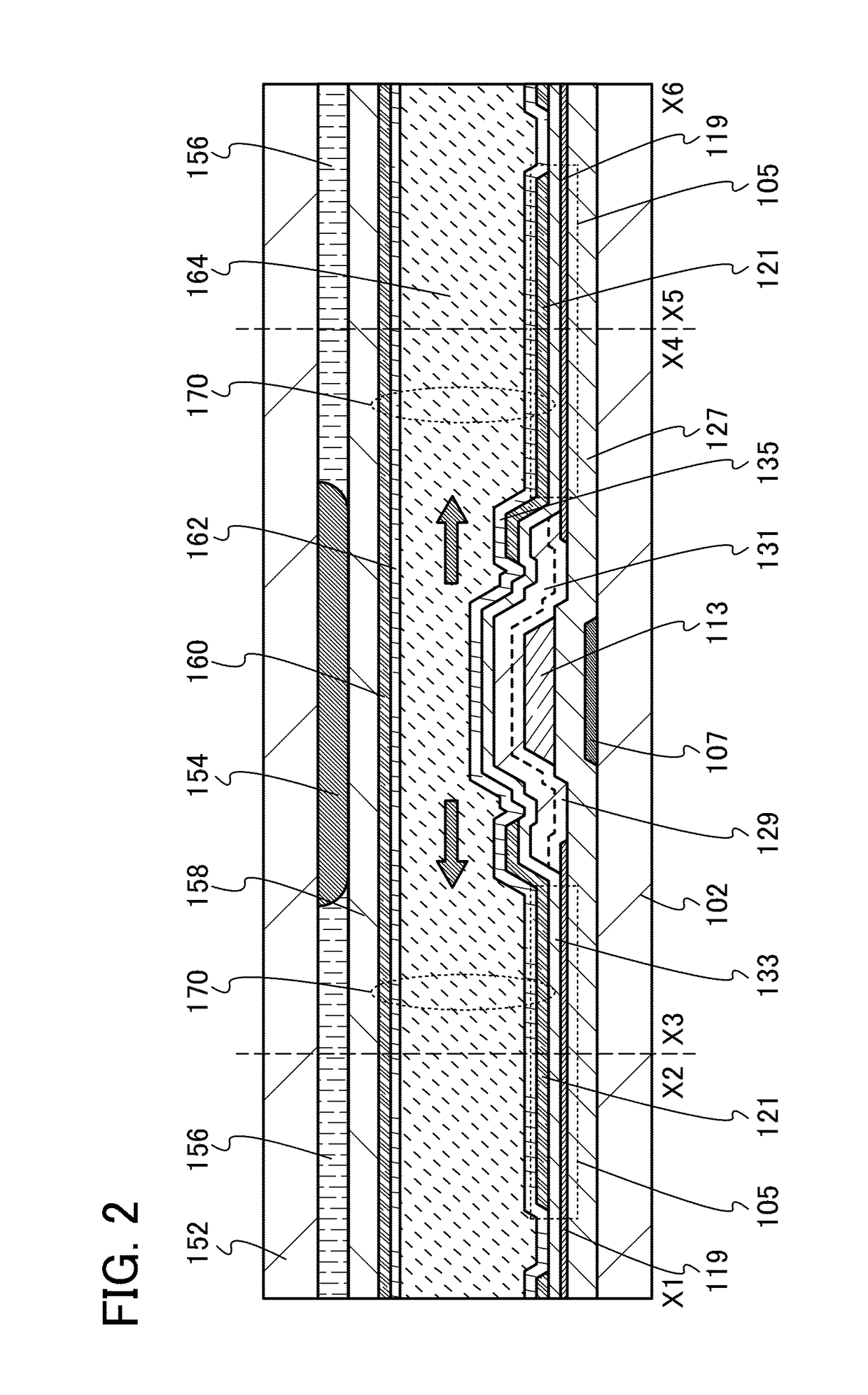
[0041]In this embodiment, a display device of one embodiment of the present invention is described with reference to FIG. 1, FIG. 2, FIG. 3, FIG. 4, FIG. 5, FIGS. 6A to 6C, FIGS. 7A to 7C, and FIGS. 8A and 8B.

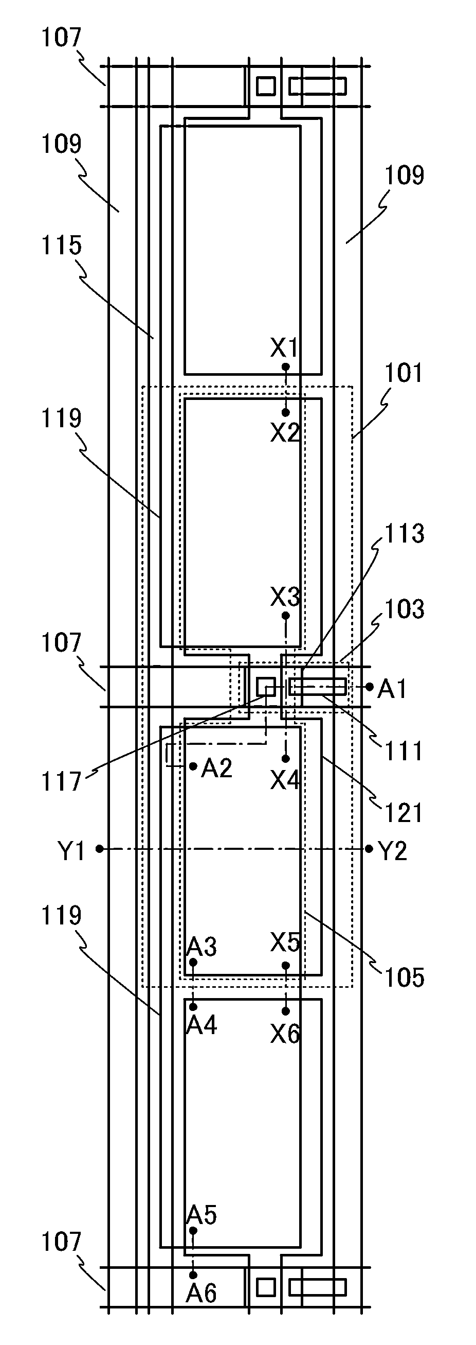
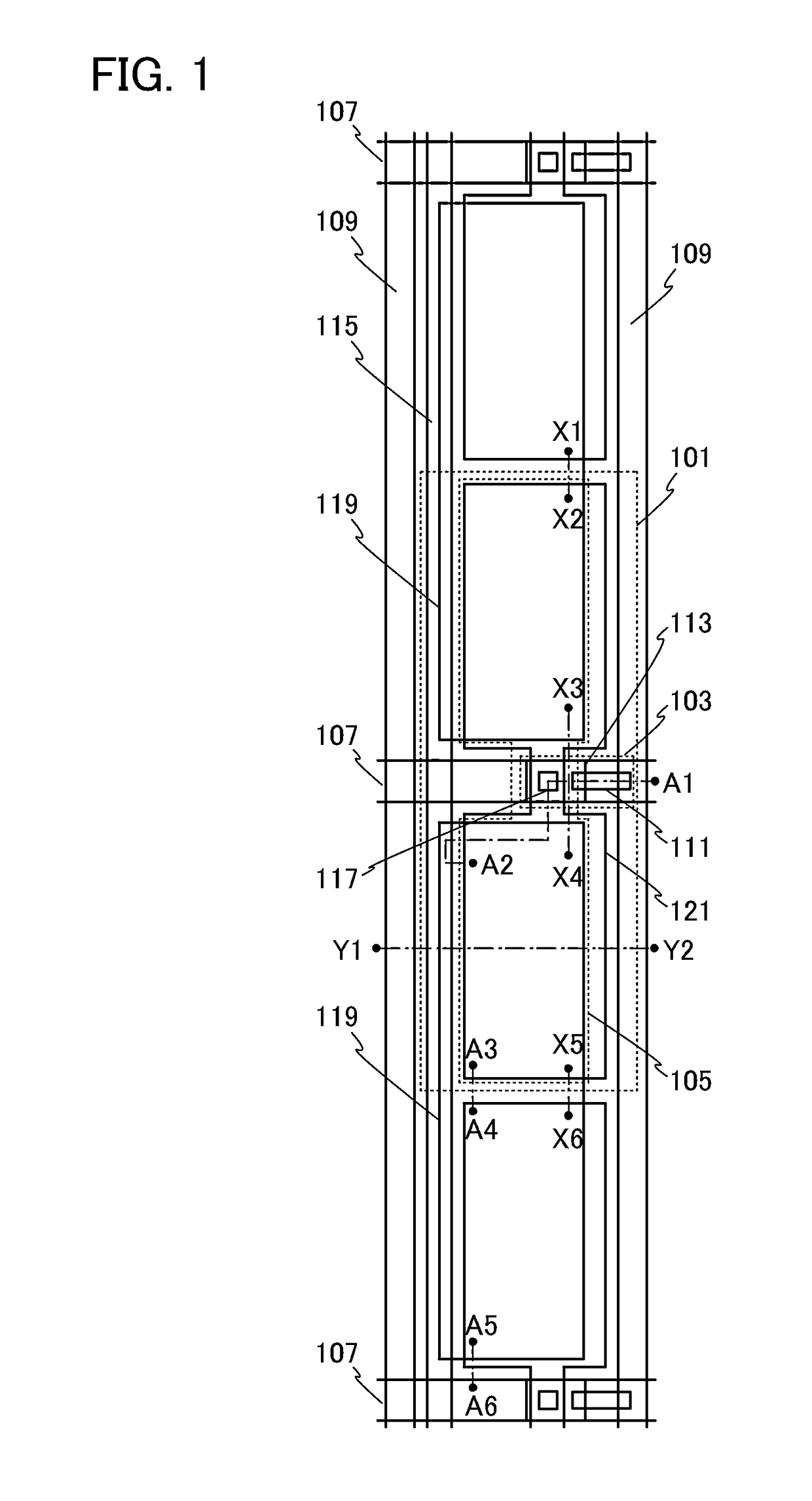
[0042]FIG. 1 is a top view of a pixel and its periphery of a display device. Note that in the top view illustrated in FIG. 1, some components are omitted in order to avoid complexity of the drawing.

[0043]In FIG. 1, a scan line 107 extends in the direction substantially perpendicular to a data line 109 (in the horizontal direction in the drawing). The data line 109 is provided to extend in the direction substantially perpendicular to the scan line 107 (in the vertical direction in the drawing). A capacitor line 115 extends in the direction substantially parallel to the data line 109.

[0044]A transistor 103 is formed to overlap with the scan line 107 and formed near a region at which the scan line 107 intersects with the data line 109. The transistor 103 includes at least a semico...

embodiment 2

[0138]In this embodiment, an example of an oxide semiconductor layer that can be used for the transistor and the capacitor of the display device described in Embodiment 1 is described.

[0139]A structure of an oxide semiconductor layer is described below.

[0140]An oxide semiconductor layer is classified roughly into a non-single-crystal oxide semiconductor layer and a single crystal oxide semiconductor layer. The non-single-crystal oxide semiconductor layer includes a c-axis aligned crystalline oxide semiconductor (CAAC-OS) film, a polycrystalline oxide semiconductor layer, a microcrystalline oxide semiconductor layer, an amorphous oxide semiconductor layer, and the like.

[0141]First, a CAAC-OS film is described.

[0142]The CAAC-OS film is one of oxide semiconductor layers including a plurality of crystal parts, and most of the crystal parts each fit inside a cube whose one side is less than 100 nm. Thus, there is a case where a crystal part included in the CAAC-OS film fits inside a cube...

embodiment 3

[0181]In this embodiment, a display device of one embodiment of the present invention is described with reference to FIGS. 13A and 13B. Note that, in this embodiment, portions that are similar to the portions in Embodiment 1 are denoted by the same reference numerals, and detailed description thereof is omitted.

[0182]The display device illustrated in FIG. 13A includes a region including pixels of display elements (hereinafter the region is referred to as a pixel portion 302), a circuit portion being provided outside the pixel portion 302 and including a circuit for driving the pixels (hereinafter the portion is referred to as a driver circuit portion 304), circuits each having a function of protecting an element (hereinafter the circuits are referred to as protection circuits 306), and a terminal portion 307. Note that the protection circuits 306 are not necessarily provided.

[0183]A part or the whole of the driver circuit portion 304 is preferably formed over a substrate over which ...


PUM

PropertyMeasurementUnit
sizesaaaaaaaaaa
sizesaaaaaaaaaa
sizesaaaaaaaaaa

Abstract

A display device having fewer alignment defects is provided. A display device having a high aperture ratio and including a capacitor with increased charge capacity is provided. A display device having a high aperture ratio, including a capacitor with large charge capacity, and having fewer alignment defects is provided. The display device includes a pixel electrode, a transistor including a light-transmitting semiconductor layer connected to the pixel electrode, and a capacitor, a scan line, and a data line connected to the transistor. The transistor is arranged to overlap with the scan line. One of electrodes of the capacitor is formed on the same surface where the semiconductor layer is formed, and is formed in a region divided by the scan lines and the data lines. The other of the electrodes of the capacitor is a pixel electrode. The pixel electrode extends so as to intersect with the scan line.

Description

BACKGROUND OF THE INVENTION[0001]1. Field of the Invention[0002]The invention disclosed in this specification and the like relates to a display device and an electronic device including the display device.[0003]2. Description of the Related Art[0004]In recent years, flat panel displays such as liquid crystal displays have been widespread. In each of pixels provided in the row direction and the column direction in a display device such as a flat panel display, a transistor serving as a switching element, a liquid crystal element electrically connected to the transistor, and a capacitor connected to the liquid crystal element in parallel are provided.[0005]As a semiconductor material of a semiconductor film of the transistor, a silicon semiconductor such as amorphous silicon or polysilicon (polycrystalline silicon) is generally used.[0006]Metal oxides having semiconductor characteristics (hereinafter referred to as oxide semiconductors) can be used for semiconductor films in transisto...

Claims


Application Information

Patent Timeline
Patent Type & Authority Patents(United States)
IPC IPC(8): G02F1/136H01L27/12G02F1/1368G02F1/1343G02F1/1362
CPCG02F1/1368H01L27/124H01L27/1255H01L27/1225G02F2201/40G02F1/136213G02F1/136286G02F1/136227G02F1/136209G02F1/133514
Inventor KUBOTA, DAISUKE
Owner SEMICON ENERGY LAB CO LTD
Why Eureka
Try Eureka