
Display device

a display device and light-emitting diode technology, applied in semiconductor devices, instruments, electrical appliances, etc., can solve the problems of low luminous efficiency of organic materials responsible for blue light, high cost of fine metal mask manufacturing, and short service life, so as to save the cost of making a display device and improve the luminous efficiency of blue sub-pixels

Active Publication Date: 2018-04-10
INNOLUX CORP
View PDF11 Cites 8 Cited by
  • Summary
  • Abstract
  • Description
  • Claims
  • Application Information

AI Technical Summary

Benefits of technology

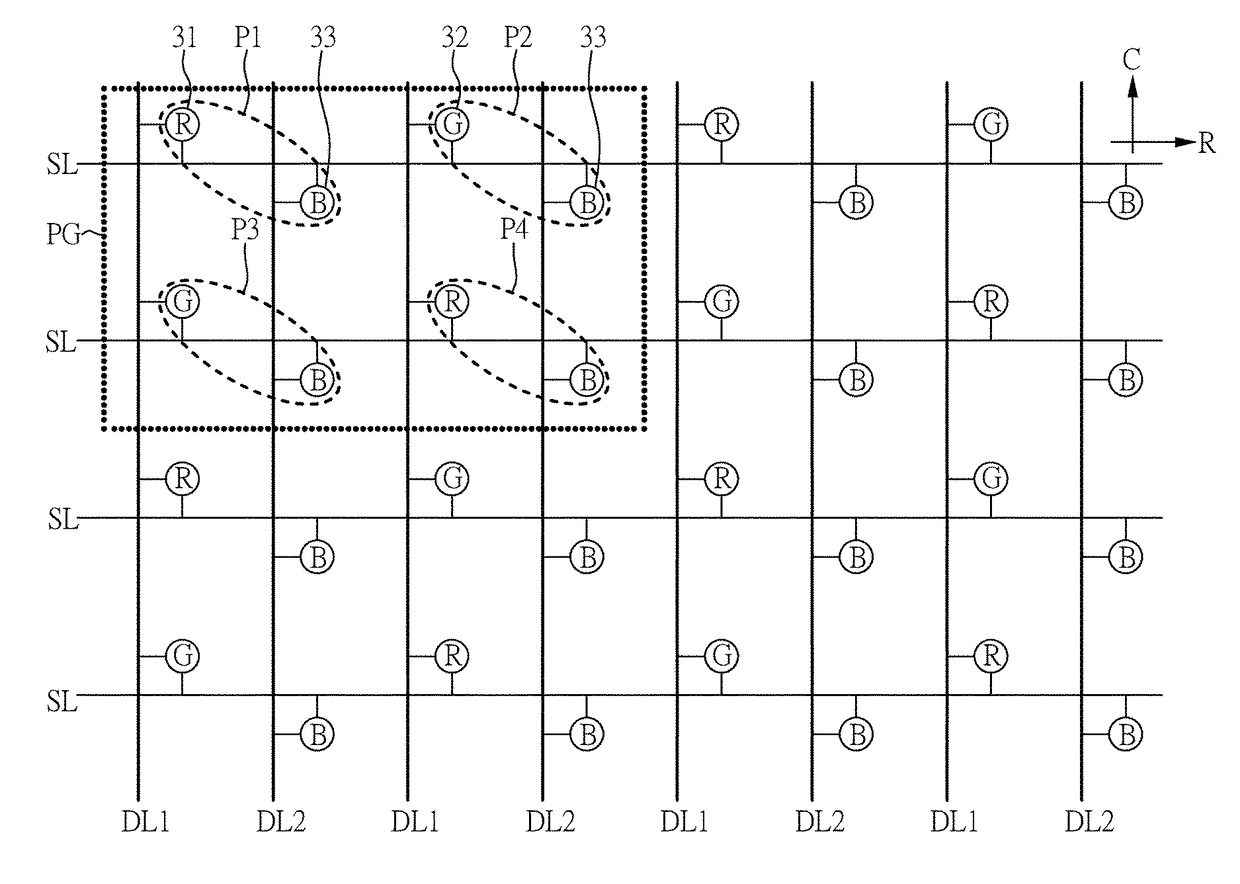
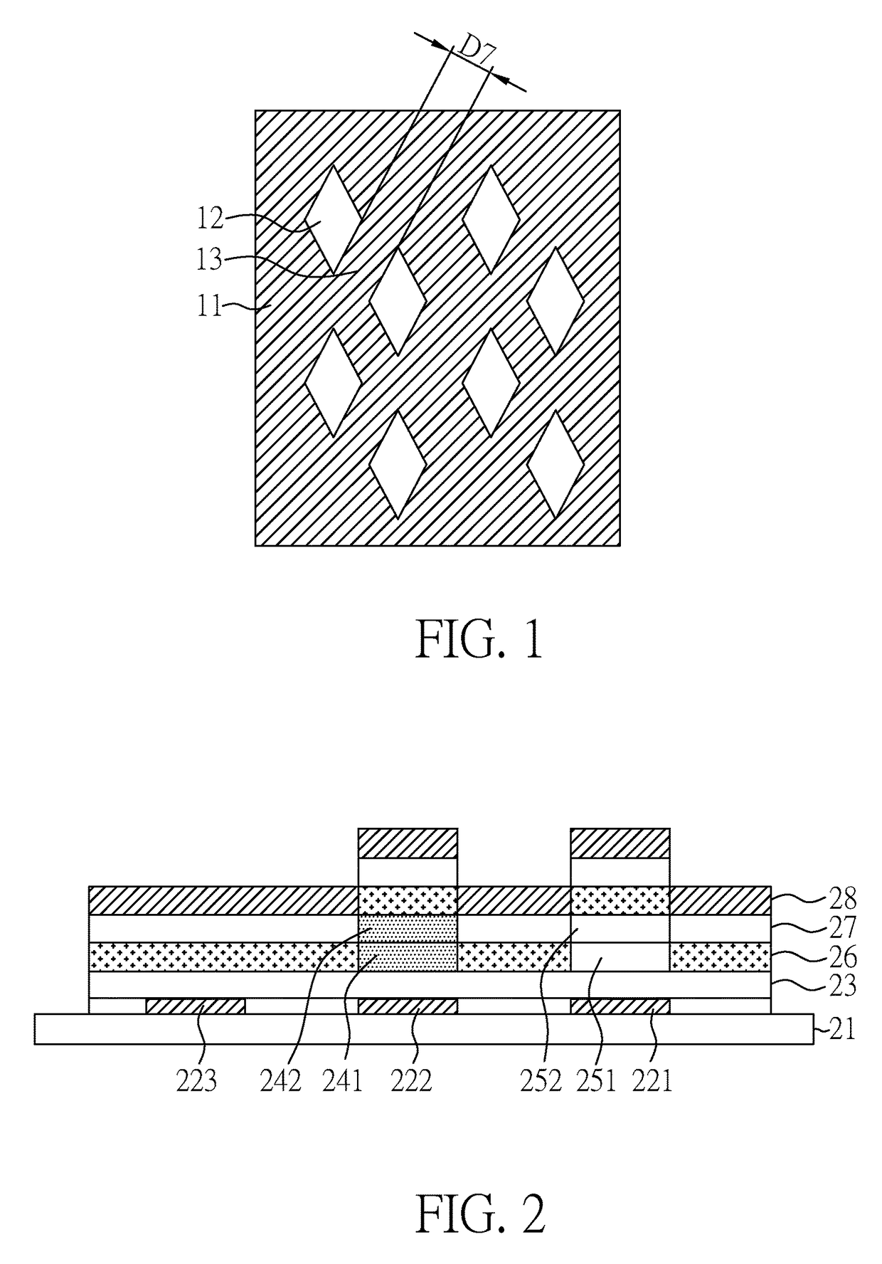
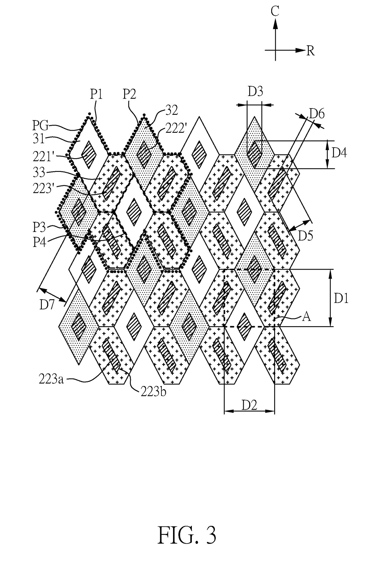
The present patent provides a display device that uses a specific arrangement of pixels to support high-resolution display. The method of making the display device requires fewer mask evaporation steps, saving costs. The blue sub-pixels, which have lower luminous efficiency, are compensated by the large percentage of blue sub-pixels in the display device. The red and green organic material layers are disposed on different electrodes, and only the formation of the red and green layers requires evaporation with metal masks of different patterns. The blue organic material layer can be made through evaporation without using another fine metal mask.

Problems solved by technology

With the development of technology related to display panels, the requirements for image fineness of display panels are more and more demanding, and this drives almost all dealers to advance their existing display panels.
However, manufacturing of a fine metal mask can be costly, and is a factor having key impact on the overall manufacturing costs of organic light-emitting diode display devices.
Apart from the above, in an organic light-emitting diode display device capable of emitting red light, green light and blue light, the organic material responsible for blue light has relatively low luminous efficiency and short service life, and this degrades the overall display quality of the organic light-emitting diode display device.

Method used


Image

  • Display device
  • Display device
  • Display device

Examples


Embodiment Construction

[0023]The following embodiments with the accompanying drawings are made to clearly exhibit the above-mentioned and other technical contents, features and effects of the present disclosure. Through the exposition by means of the specific embodiments, people would further understand the technical means and effects the present disclosure adopts to achieve the above-indicated objectives. Moreover, as the contents disclosed herein should be readily understood and can be implemented by a person skilled in the art, all equivalent changes or modifications which do not depart from the concept of the present disclosure should be encompassed by the appended claims.

[0024]Furthermore, the ordinals recited in the specification and the claims such as “first”, “second” and so on are intended only to describe the elements claimed and imply or represent neither that the claimed elements have any preceding ordinals, nor that sequence between one claimed element and another claimed element or between s...


PUM


Abstract

A display device is disclosed, which includes: a pixel group including a first pixel having a red sub-pixel and a blue sub-pixel; a second pixel having a green sub-pixel and a blue sub-pixel; a third pixel having a green sub-pixel and a blue sub-pixel; and a fourth pixel having a red sub-pixel and a blue sub-pixel. The first pixel is adjacent to the second pixel in a row direction. The first pixel is adjacent to the second pixel in a column direction. The fourth pixel is diagonal to the first pixel, and the fourth pixel is adjacent to the second pixel and the third pixel. In the pixel group, the blue sub-pixels are quantitatively more than the red sub-pixels, and the blue sub-pixels are quantitatively more than the green sub-pixels.

Description

CROSS REFERENCE TO RELATED APPLICATION[0001]This application claims the benefits of the Taiwan Patent Application Serial Number 105108781, filed on Mar. 22, 2016, the subject matter of which is incorporated herein by reference.BACKGROUND[0002]1. Field of the Disclosure[0003]The present disclosure relates to display devices, and more particularly to an organic light-emitting diode display device wherein red, green and blue sub-pixels are arranged in a novel manner.[0004]2. Description of Related Art[0005]With the development of technology related to display panels, the requirements for image fineness of display panels are more and more demanding, and this drives almost all dealers to advance their existing display panels. Particularly, the growth of 4K2K panels and hand-held display devices with high PPI (pixels per inch) resolution, such as mobile phones, tablets, etc., further confirms the trend in the panel industry toward even higher resolution, which means more pixels have to be...

Claims


Application Information

Patent Timeline
Patent Type & Authority Patents(United States)
IPC IPC(8): H01L27/32H01L51/00G09G3/3233G09G5/02H10K99/00
CPCH01L27/3218G09G3/3233G09G5/02H01L51/0011H01L27/3216H01L27/3276H01L27/3213H10K59/351H10K59/353H10K59/131H10K59/352H10K71/166
Inventor HSU, YI-HUATSENG, MING-CHUN
Owner INNOLUX CORP
Learn More