Trench MOSFET with on-resistance reduction

a technology of mosfet and drain, which is applied in the field of cell structure and fabrication process of power semiconductor devices, can solve the problems of poor metal coverage, unreliable electrical contact, and difficulty, and achieve the effect of reducing drain and source resistance, shortening p-body anneal or diffusion, and reducing drain-source resistan

Inactive Publication Date: 2011-01-13
FORCE MOS TECH CO LTD
View PDF4 Cites 40 Cited by
  • Summary
  • Abstract
  • Description
  • Claims
  • Application Information

AI Technical Summary

Benefits of technology

[0010]Another aspect of the present invention is to further reduce the drain and source resistance significantly by forming P-body with medium or high energy Ion Implantation or combination of both energies Ion Implantation. This method of Ion Implantation at medium or high energy can shorten P-body anneal or diffusion. Incorporating with Phosphorus substrate with resistivity lower than 2.0 mohm-cm, the drain-source resistance is hence reduced significantly. Thus drift resistance and substrate resistance are also reduced.
[0011]Another aspect of the present invention is the new metal scheme of Ti / TiN / W / Ti thick front metal or Co / Ti / TiN / W thick front metal due to the use of Ti / TiN or Co / TiN as alternative as barrier layer discussed above which will provide good ohmic contact, and further reduce the contact resistance.
[0012]Another aspect of the present invention is the champagne cup shaped contact, which has two advantages. One is the forming the stepwise structure for better ohmic contact, the other is there is no need to etch off Ti / TiN or Co / TiN after the tungsten is etched back which is benefit for the saving of fabricating cost.
[0013]Another aspect of the present invention is improved device ruggedness with the sloped source trench contact (60˜90 degree respect to epi surface) and optimum space between trench and contact (0.1˜0.3 um) without impacting drain-source resistance. Because of the P+ region touching channel region, the drain-source resistance is significantly increased if the contact space is smaller than 0.1 um, and if the space is greater than 0.3 um, the avalanche capability is degraded due to a parasitic N+P / N is triggered on. Those two aspects sufficiently indicate the present invention is deserved to be put into application.
[0014]Briefly, in a preferred embodiment, the present invention discloses a trenched metal oxide semiconductor field effect transistor (MOSFET) cell that includes a trenched gate surrounded by a source region encompassed in a body region above a drain region disposed on a bottom surface of a Phosphorus substrate with a resistivity lower than 2.0 mohm-cm, and the said P-body region is implanted by using medium or high energy Ion Implantation to assurance the drain-source resistance is reduced. The MOSFET cell further includes a source-body contact trench opened with champagne cup shape and surrounded by a Ti / TiN or Co / TiN as alternative as barrier layer and filled with contact metal plug. A body-resistance reduction region P+ doped with body-doped is formed to surround the source-body contact trench to reduce a body-region resistance between the source-body contact metal and the trenched gate to improve an avalanche capability. In a preferred embodiment, the contact metal plug further comprises a Ti / TiN or Co / TiN barrier layer surrounding a tungsten core as a source-body contact metal. In another preferred embodiment, the MOSFET cell further includes an insulation layer compromising BPSG or PSG and undoped SRO (silicon rich oxide) covering a top surface over the MOSFET cell wherein the source body contact trench is opened through the insulation layer. And, the MOSFET cell further includes a thin resistance-reduction conductive layer such as Ti or Ti / TiN disposed on a top surface covering the insulation layer and contacting the contact metal plug whereby the resistance-reduction conductive layer having a greater area than a top surface of the contact metal plug for reducing a source-body resistance. In another preferred embodiment, the MOSFET cell further includes a thick front metal layer disposed on top of the resistance-reduction layer for providing a contact layer for a wire or wireless bonding package. In another preferred embodiment, the sloped source trench contact has a degree of 60˜90 respect to epi surface and the optimum space between trench and contact is 0.1˜0.3 um, therefore the device ruggedness is improved without impacting drain-source resistance.
[0015]This invention further discloses a method for manufacturing a trenched metal oxide semiconductor field effect transistor (MOSFET) cell comprising a step of forming said MOSFET cell with a trenched gate surrounded by a source region encompassed in a body region above a drain region disposed on a bottom surface of a Phosphorus substrate. In a preferred embodiment, the step of implanting the P-body region is a step of Ion Implantation with medium or high energy in a epi formed above the Phosphorus substrate which has a resistivity lower than 2.0 mohm-cm. The method further includes a step of covering the MOSFET cell with an insulation layer and applying a contact mask for opening a source-body contact trench. In a preferred embodiment, the step to form a source-body contact with stepwise sidewalls is applying a wet oxide etch to etch the insulation layer and depositing Ti / TiN or Co / TiN layer and there is or no Ti / TiN or Co / TiN etch off step after the W etch back. The method further includes a step of forming a body-resistance-reduction-dopant region by implanting a body-resistance-reduction-dopant in the body region immediately near the source-body contact trench whereby an avalanche capability of the MOSFET cell is enhanced. In a preferred embodiment, the step of implanting the body-resistance-reduction-dopant is a step of implanting a dopant of a same conductivity type as a body dopant doped in the body region. In a preferred embodiment, the step of forming the body-resistance-reduction region further includes a step of forming the body-resistance-reduction region surrounding a bottom portion of the source-body contact trench.

Problems solved by technology

Conventional technologies of forming aluminum metal contact to the N+ source and P-well formed in the P-body regions in a semiconductor device is encountering a technical difficulty of poor metal coverage and unreliable electrical contact when the cell pitch is shrunken.
The technical difficulty is especially pronounced when a metal oxide semiconductor field effect transistor (MOSFET) cell density is increased above 200 million cells per square inch (200 M / in2) with the cell pitch reduced to 1.8 um or to even a smaller dimension.
The metal contact space to both N+ source and P-well in the P-body regions for cell density higher than 200 M / in2 is less than 1.0 um, resulting in poor metal step coverage and high contact resistance to both N+ and P-body region.
The device performance is adversely affected by these poor contacts and the product reliability is also degraded.
Another limitation of the MOSFET device structure in the prior art is the poor contact resistance which partly caused by the poor contact between W and Al alloys 16.
In another respect, considering the trench contact is not stepwise, it offers less contact area between W and Al alloys 16, which causing further poor contact resistance.
Both aspects discussed above bring a high drain-source resistance which will lead to a power wastage.

Method used


Image

  • Trench MOSFET with on-resistance reduction
  • Trench MOSFET with on-resistance reduction
  • Trench MOSFET with on-resistance reduction

Examples


Embodiment Construction

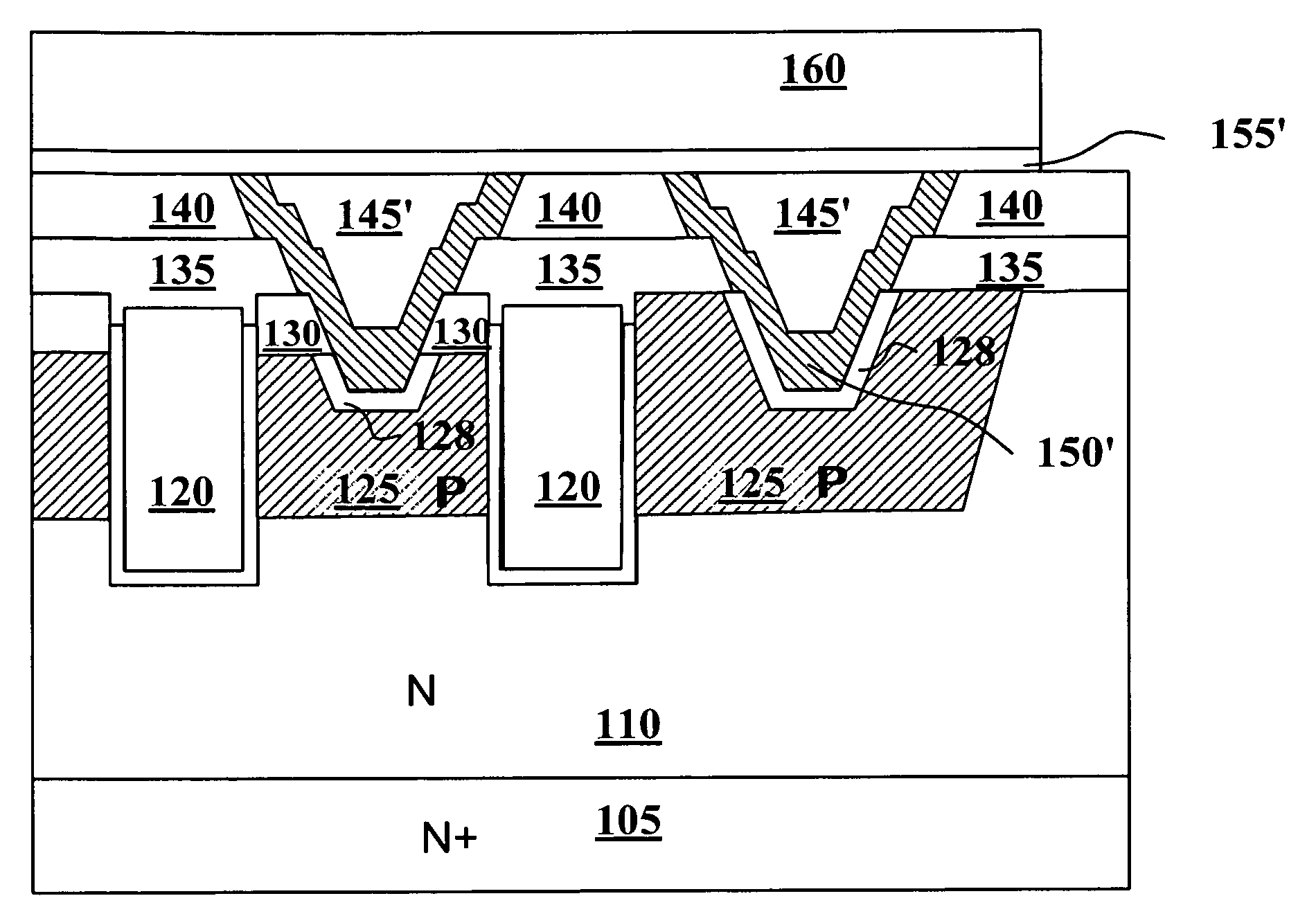
[0023]Please refer to FIG. 3 for preferred an embodiment of this invention where a metal oxide semiconductor field effect transistor (MOSFET) device 100 is formed on a Phosphorus N+ substrate 105 formed with an N epitaxial layer 110. The MOSFET 100 includes a trenched gate 120 disposed in a trench with a gate insulation layer formed over the walls of the trench. A body region 125 that is doped with a dopant of second conductivity type, e.g., P-type dopant, extends between the trenched gates 120.

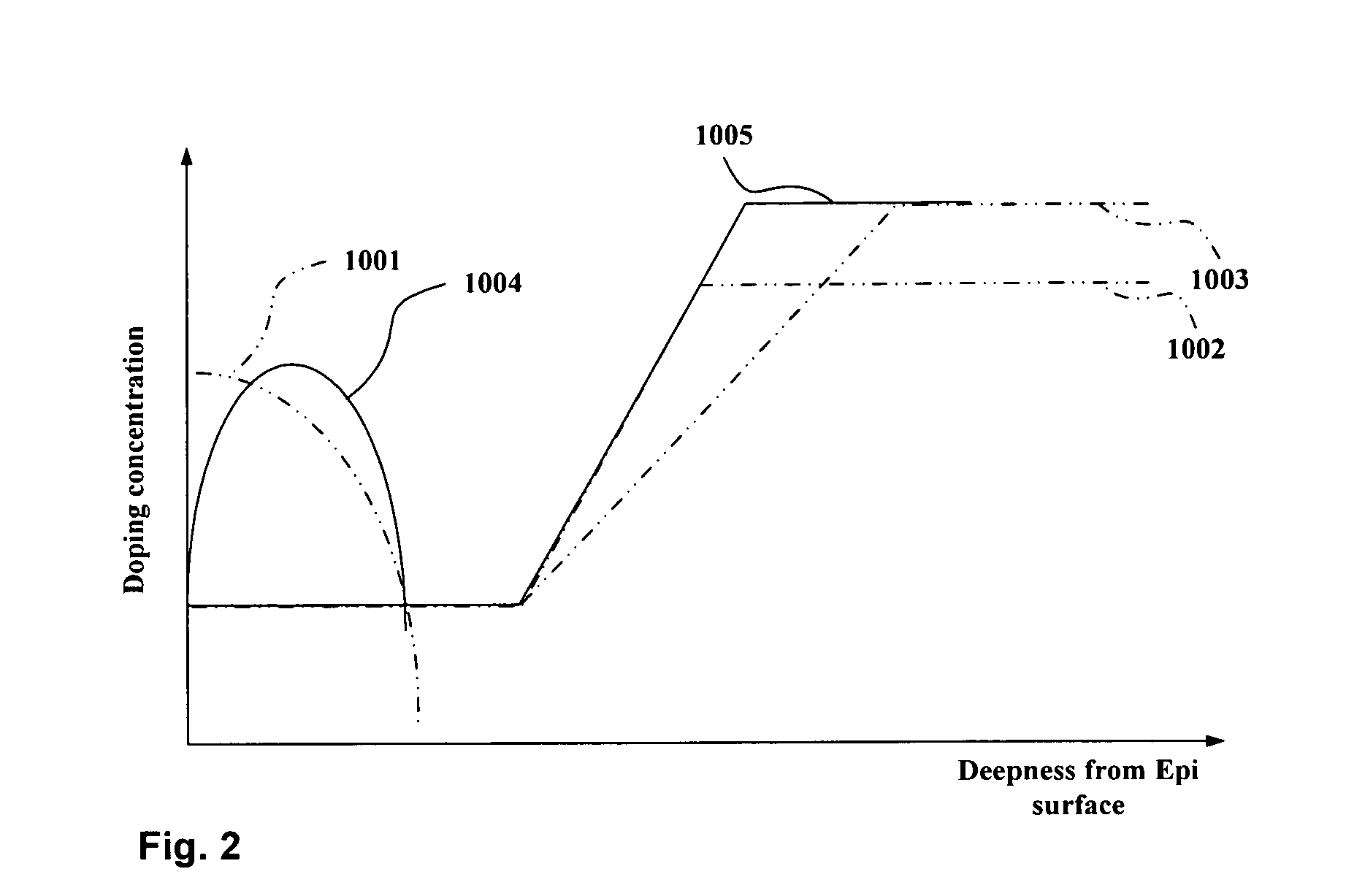
[0024]For the purpose of reduce the drain-source resistance significantly, the substrate of this invention is Phosphorus substrate as mentioned which has a resistivity lower than 2.0 mohm-cm. On the other hand, P-body region is implemented by medium or high energy (100˜400 KeV) Ion Implantation and followed by Anneal at 1000˜1100 C to form a retrograded P-body / N-Epi junction (1004 in FIG. 2) with thinner Epi. And incorporated with the Phosphorus substrate (1005 in FIG. 2), the impact of drift...


PUM

PropertyMeasurementUnit
refractive indexaaaaaaaaaa
temperatureaaaaaaaaaa

Abstract

A trench MOSFET with on-resistance reduction comprises a trenched gate surrounded by a source region encompassed in a body region above a drain region disposed on a bottom surface of a substrate, wherein the said MOSFET further comprises a plurality of source-body contact trenches opened relative to a top surface into said source and body regions and each of the source-body contact trenches is filled with a contact metal plug as a source-body contact; a insulation layer covered over the top of the trenched gate, the body region and the source region; a front metal layer formed on a top surface of the MOSFET; wherein a low-resistivity phosphorus substrate and retrograded P-body formed by medium or high energy Ion Implantation to reduce Rds contribution from substrate and drift region.

Description

BACKGROUND OF THE INVENTION[0001]1. Field of the Invention[0002]This invention relates generally to the cell structure and fabrication process of power semiconductor devices. More particularly, this invention relates to a novel and improved cell structure and improved process of fabricating a trenched semiconductor power device with reduced drain-source resistance and better metal step coverage.[0003]2. The Prior Arts[0004]Conventional technologies of forming aluminum metal contact to the N+ source and P-well formed in the P-body regions in a semiconductor device is encountering a technical difficulty of poor metal coverage and unreliable electrical contact when the cell pitch is shrunken. The technical difficulty is especially pronounced when a metal oxide semiconductor field effect transistor (MOSFET) cell density is increased above 200 million cells per square inch (200 M / in2) with the cell pitch reduced to 1.8 um or to even a smaller dimension. The metal contact space to both N+...

Claims


Application Information

Patent Timeline
Patent Type & Authority Applications(United States)
IPC IPC(8): H01L29/78H01L21/336
CPCH01L29/1095H01L29/41766H01L29/456H01L29/66727H01L29/66734H01L29/7811H01L29/7813
Inventor HSIEH, FU-YUAN
Owner FORCE MOS TECH CO LTD
Why Eureka
Try Eureka