Semiconductor device and method of manufacturing the same

a semiconductor device and semiconductor technology, applied in semiconductor devices, semiconductor/solid-state device details, electrical devices, etc., can solve the problems of deterioration of noise characteristic due to substrate resistance, conspicuous noise characteristic, heat noise caused by substrate resistance, etc., to achieve high gain, reduce heat noise, improve noise characteristic of semiconductor devices

Inactive Publication Date: 2005-03-29
KK TOSHIBA
View PDF19 Cites 0 Cited by
  • Summary
  • Abstract
  • Description
  • Claims
  • Application Information

AI Technical Summary

Benefits of technology

The semiconductor device according to the present invention includes the low-resistance layer provided under the interconnection extending from the signal input, whereby the influence of the substrate resistance is suppressed by this low-resistance layer, the heat noises caused by the substrate resistance can be reduced, and the noise characteristic of the semiconductor device can also be improved.
If the silicide layer given the same potential as that of the substrate or the well is used as the low-resistance layer, an ideal low-resistance shield is easily obtained, and it is feasible to acquire a high gain due to the decrease in the inter-layer capacitance and to attain the simplified interconnection.

Problems solved by technology

Then, thermal noises caused by this substrate resistance R1 enter the input stage of the transistor via the inter-layer film capacitance C1, resulting in deterioration of the noise characteristic.
In particular, the deterioration of the noise characteristic due to the substrate resistance becomes conspicuous in a MOSFET with a high gate input impedance.

Method used


Image

  • Semiconductor device and method of manufacturing the same
  • Semiconductor device and method of manufacturing the same
  • Semiconductor device and method of manufacturing the same

Examples


first embodiment

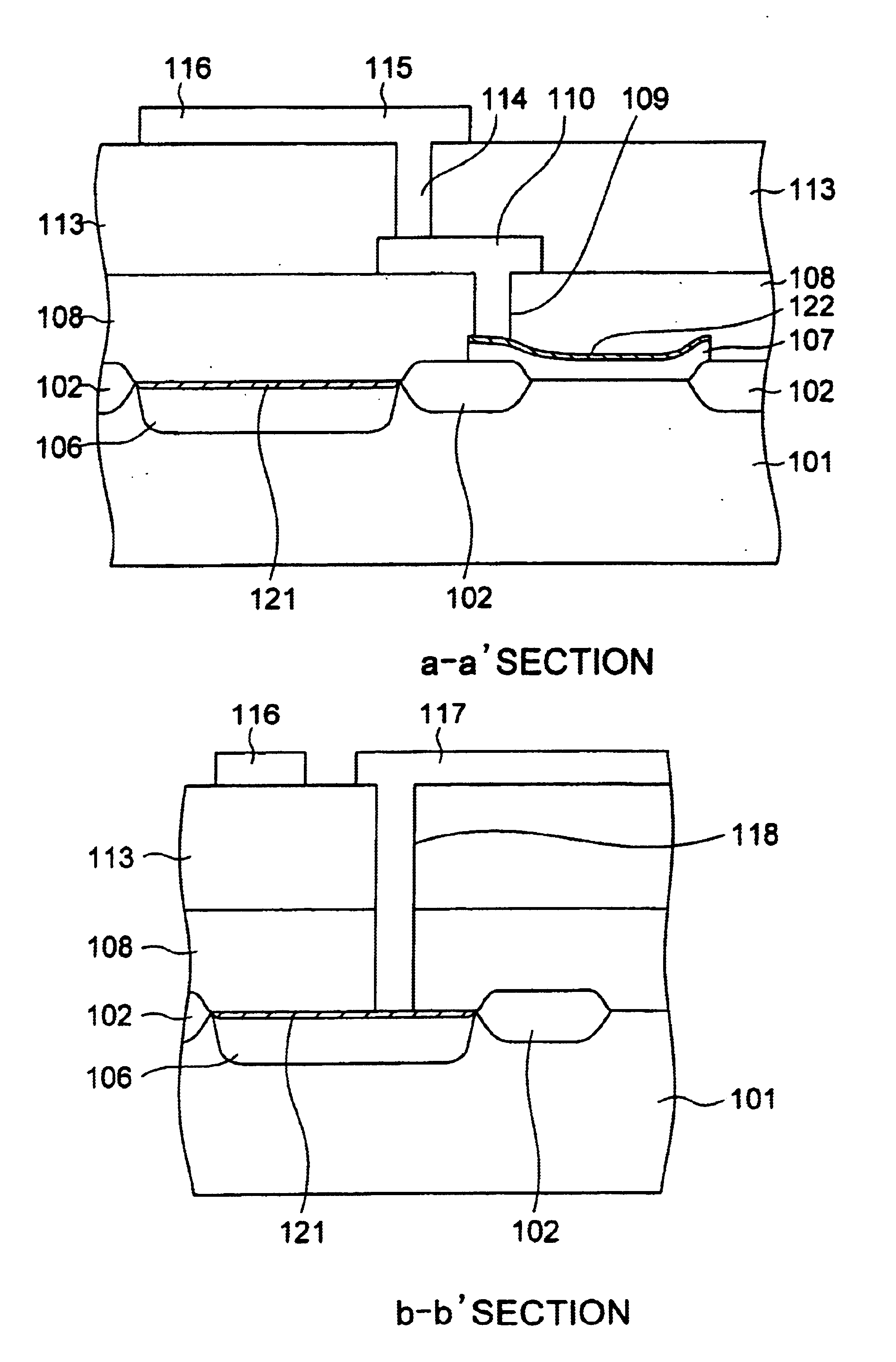
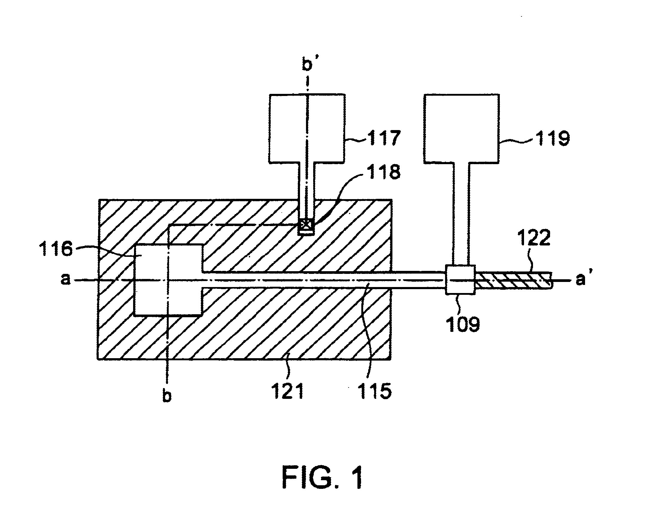
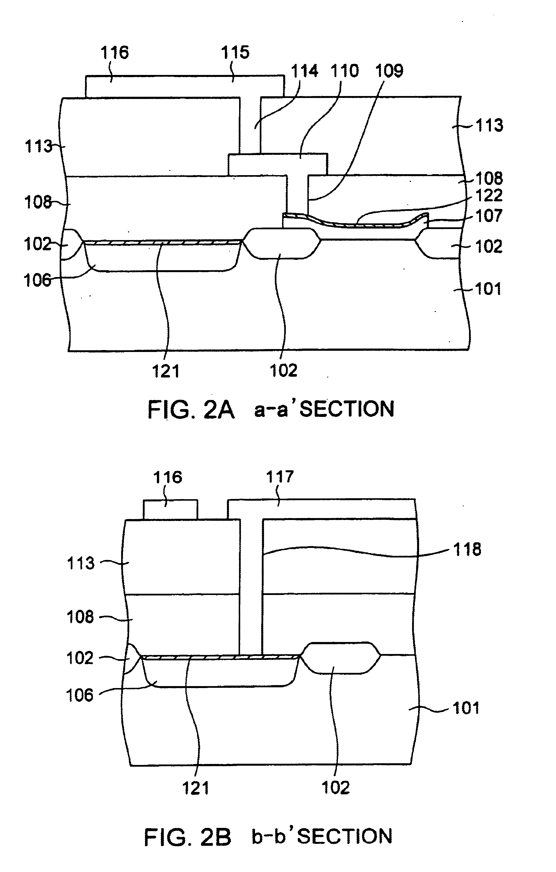
FIG. 1 is a plan view showing a layout of a semiconductor device in the present invention. FIG. 2A shows a cross sectional view of the semiconductor device along the line a-a′ in FIG. 1 and FIG. 2B shows a cross sectional view of the semiconductor device along the line b-b′ in FIG. 1. FIGS. 1, 2A and 2B show a gate area of a MOSFET at an input stage of a low-noise amplifier. FIG. 11 shows a plurality of MOSFETs arranged in a comb-like shape to form an amplifier stage. Throughout FIGS. 1, 2A and 2B, the elements corresponding to those in the prior art explained in FIGS. 9 and 10 are marked with the reference numerals 100s.

At the surface part of a silicon substrate 101, a device region and a substrate potential take-out region enveloped and isolated by a field oxide layer 102. At the surface part of the substrate surface in the substrate potential take-out region is formed with an impurity high-concentration diffused region 106, having the same conductivity type as that of a well, for...

second embodiment

FIG. 5 is a plan view showing a layout of the semiconductor device in the present invention. FIGS. 6A and 6b are sectional views of the device taking along sectional lines c-c′ and d-d′, respectively. The same elements as those in FIGS. 1, 2A and 2B are marked with the same reference numerals.

A difference between the second embodiment and the first embodiment is that the silicide layer 121 in the substrate potential take-out region is disposed under the interconnection take-out pad as well as under the interconnection in the gate area of the MOSFET at the input stage of the low-noise amplifier in the first embodiment, however, a silicide layer 142 is disposed on a polysilicon layer 141 provided on an oxide layer (field oxide layer) for a device isolation in the second embodiment. The polysilicon layer 141 can be actualized by its being composed of the same layer as that of the gate electrode, and, in this case, the layers are simultaneously formed by patterning.

Moreover, the substra...


PUM


Abstract

The semiconductor device has a low-resistance layer provided under the interconnection extending from the singal input to a gate of MOSFET. The low-resistance layer suppresses the influence of the substrate resistance and the noise characteristic of the semiconductor device can also be improved. The low-resistance layer can be provided on a surface of the substrate or a polysilicon interconnection.

Description

BACKGROUND OF THE INVENTIONThe present invention relates generally to a semiconductor device, and more particularly to a semiconductor device suited to a low-noise type transistor, for example, a MOSFET and an integrated circuit using the same.A low-noise characteristic is especially required of, e.g., an amplifier circuit among a variety of circuits included in a semiconductor device.A comb-shape structured transistor has hitherto been used as a transistor in which the above low-noise characteristic is actualized.This comb-shape structured transistor having, as illustrated in a plan view of FIG. 9, source regions 3 and drain regions 4 which have alternately been formed with strips of gate electrodes 7 extending therebetween, is configured as a whole in a laterally elongate rectangular shape. That is, the plurality of gate electrodes 7 alternately extend across long sides of this rectangle, and contact holes 9 and electrodes 10 are so provided as to connect the adjacent gate electro...

Claims


Application Information

Patent Timeline
Patent Type & Authority Patents(United States)
IPC IPC(8): H01L21/70H01L21/00H01L21/02H01L21/3205H01L21/8234H01L27/085H01L27/088H01L27/01H01L27/04H01L21/336H01L23/52H01L29/06H01L29/10H01L29/40H01L29/45H01L29/49H01L29/78
CPCH01L21/823475H01L27/088H01L29/0692H01L29/1087H01L29/402H01L29/66492H01L29/78H01L29/7833H01L29/456H01L29/4933H01L2924/0002H01L29/665H01L2924/00H01L27/04
Inventor MORIFUJI, EIJI
Owner KK TOSHIBA
Why Eureka
Try Eureka