Complex filter circuit

a filter circuit and complex technology, applied in the field of filter circuits, can solve the problems of circuit elements increasing in number and chip size, difficult to maintain flat characteristic in the passband, and increasing the number of circuit elements, so as to reduce the order of filter in the present invention, reduce current consumption, and reduce chip area

Inactive Publication Date: 2007-08-09
NEC ELECTRONICS CORP
View PDF5 Cites 15 Cited by
  • Summary
  • Abstract
  • Description
  • Claims
  • Application Information

AI Technical Summary

Benefits of technology

[0083]In accordance with the present invention, the desired attenuation characteristic can be implemented by a filter of the lowest order. The reason for this is that the frequency characteristic of the filter can be made the desired attenuation characteristic in the entirety of the circuit inclusive of amplifying means within the filter.
[0084]In accordance with the present invention, current consumption can be reduced. The reason is that the order of the filter in the present invention can be minimized.
[0085]In accordance with the present invention, chip area can be reduced. The reason is that implementation in the present invention is possible with a filter of the minimum order inclusive of amplifying means.
[0086]In accordance with the present invention, an excellent noise characteristic can be obtained. The reason is that in the present invention, noise that has been amplified by amplifying means can be attenuated in a filter section of a latter stage.

Problems solved by technology

The first problem is that the flat characteristic in a passband cannot be maintained.
These factors make it particularly difficult to maintain a flat characteristic in the passband.
The second problem is that since it is necessary to raise the order of the filter in order to obtain the desired attenuation characteristic, the circuit elements increase in number and chip size increases.
The third problem is an increase in current consumed by the filter circuit.

Method used


Image

  • Complex filter circuit
  • Complex filter circuit
  • Complex filter circuit

Examples


first embodiment

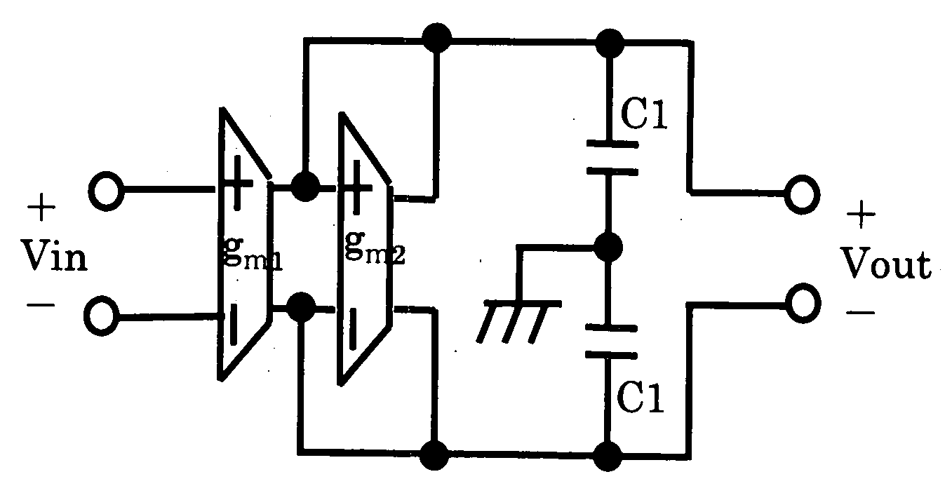
[0203]In a gm-C filter, capacitance C is transformed to inductance L using a gyrator, and an LCR filter is transformed to an OTA-C filter, namely a so-called gm-C filter. However, in the case of a floating L, four OTAs and one capacitor become necessary, the number of elements is large and it is difficult to reduce circuit current.

[0204]If the above-described biquad method is used, this portion can be eliminated and four OTAs are required per second-order filter. Accordingly, this problem is particularly serious in a complex filter in which LPFs are required in the two channels of I and Q.

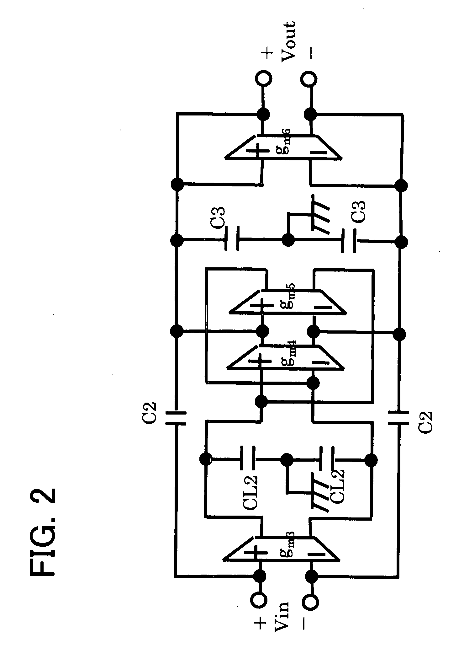
[0205]If the elliptic RLC ladder LPF shown in FIG. 16 is transformed to a complex filter, the result will be as shown in FIG. 4.

[0206]Admittance YC2 of a series branch (L2, −jR2, C2, −jG2) of the complex third-order elliptic filter shown in FIG. 4 is as follows:

YC2(s)=1sL2-jR2+sC2-jG2=s2L2C2-js(R2C2+L2G2)+1-R2G2sL2-jR2(70)

[0207]If an admittance equivalent to YC2(S) can be implemented solely by an i...

second embodiment

[0238]As illustrated in the first embodiment, the elliptic capacitor and the gm value of the coupler between the I and Q capacitors must take on fractional values of C2= 1 / 43, gm6=0.157, respectively.

[0239]For the purpose of simplifying the circuitry, it is necessary to consider eliminating the coupler of the elliptic capacitors between I, Q and also the elliptic capacitor.

[0240]The coupler of the elliptic capacitors between the I, Q capacitors operates in such a manner that the transmission zero point of the complex filter on the low-frequency side thereof will become a point on the negative (minus) side.

[0241]Further, the transmission zero point always appears on the side of low frequency owing to the admittance transformation.

[0242]It will be understood from FIG. 11 that if a frequency shift ω0 along the frequency axis can be set at will, then there will be no problem even if the transmission zero point of the complex filter on the low-frequency side thereof is zero frequency.

[02...


PUM


Abstract

Disclosed is a complex elliptic filter having an order of three or higher which receives two differential signals that differ in phase from each other by 90 degrees are applied and outputs two differential signals that differ in phase from each other by 90 degrees. The complex filter circuit has internally at least two circuit blocks that include a capacitor connected in series with a coupler (gyrator). The complex filter is a third-order inverse Chebychev filter having an equiripple stopband of 40-dB attenuation amount. Alternatively, the coupler (gyrator) between elliptic capacitors is removed. Alternatively, the elliptic capacitors are made substantially equal to the capacitor arranged in parallel therewith. Alternatively, the gm value of an OTA and the capacitance value are each in an integral ratio represented substantially by a geometric progression of 2.

Description

FIELD OF THE INVENTION[0001]This invention relates to a filter circuit and, more particularly, to an on-chip filter circuit integrated on an LSI chip.BACKGROUND OF THE INVENTION[0002]Conventionally, receivers use a Hartley-type image rejection mixer or a Weaver-type image rejection mixer for the purpose of removing signal components from the image frequency band.[0003]The receivers in low-end radios have recently come to employ a receiving scheme referred to as “low-IF” which has the ability to lower IF frequency with a single superheterodyne and which readily lends itself to LSI fabrication and signal processing.[0004]Since the IF frequency is low, however, image noise cannot be eliminated by an RF filter inserted in front of the mixer. For this reason, a complex filter circuit has come to be used as the filter circuit for extracting the IF signal from the mixer output signal by employing quadrature demodulation for performing signal processing upon producing a difference in phase ...

Claims


Application Information

Patent Timeline
Patent Type & Authority Applications(United States)
IPC IPC(8): H03K5/00
CPCH03H11/04H03H11/08H03H11/1247H03H2011/0494H03H11/1252H03H11/0433H03H11/045
Inventor KIMURA, KATSUJI
Owner NEC ELECTRONICS CORP
Why Eureka
Try Eureka