Semiconductor device

Active Publication Date: 2018-05-08
SAMSUNG ELECTRONICS CO LTD
View PDF18 Cites 2 Cited by
  • Summary
  • Abstract
  • Description
  • Claims
  • Application Information

AI Technical Summary

Benefits of technology

This patent describes a semiconductor device that uses different materials in its channel layers for PMOS and NMOS transistors, which results in better performance.

Problems solved by technology

The reduction in the electric charge mobility in the channel may hinder improvement in saturation current of the transistor.

Method used


Image

  • Semiconductor device
  • Semiconductor device
  • Semiconductor device

Examples


Embodiment Construction

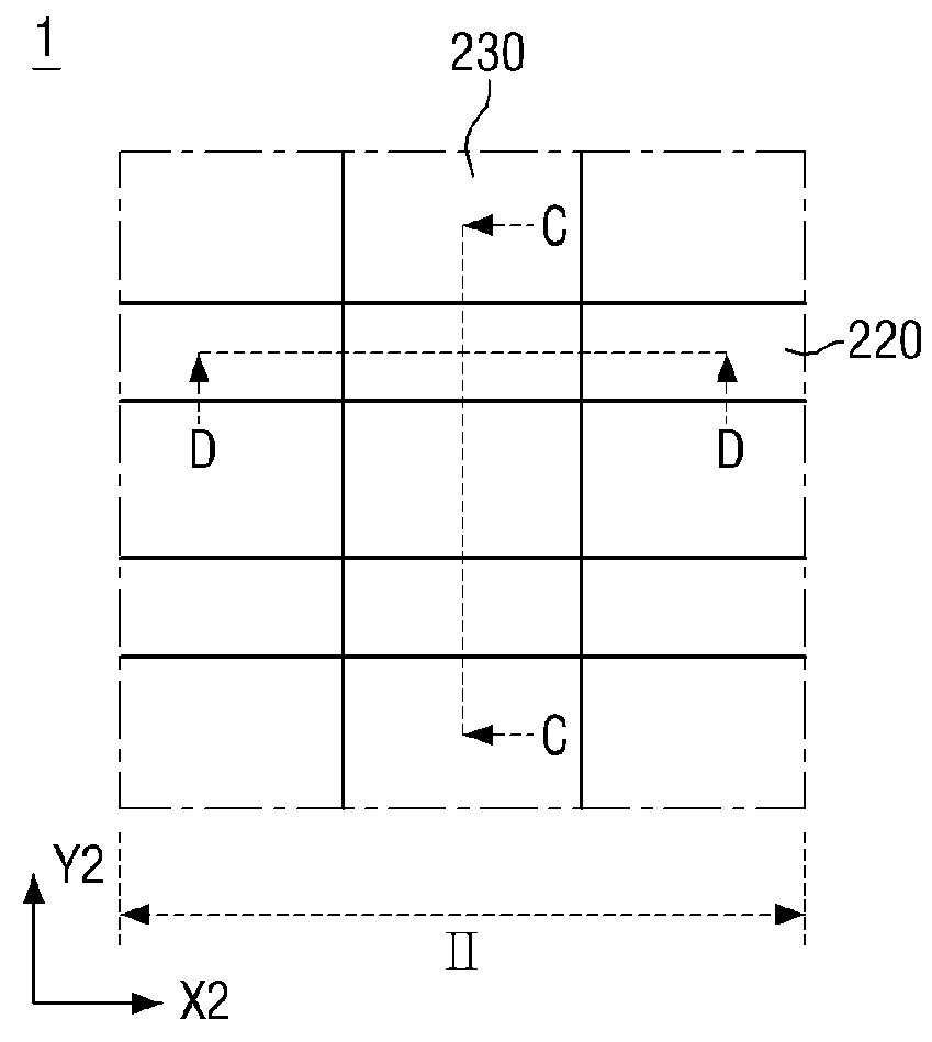
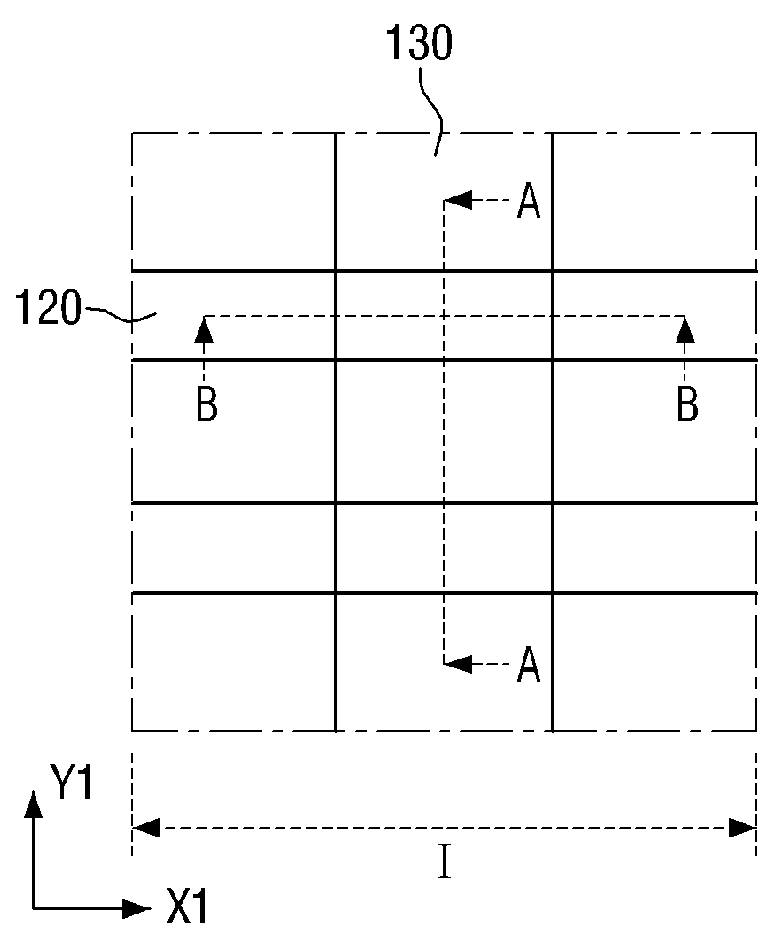
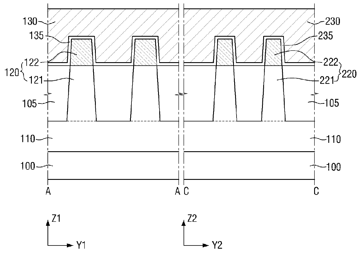
[0068]One or more example embodiments will be described in detail with reference to the accompanying drawings. Example embodiments, however, may be embodied in various different forms, and should not be construed as being limited to only the illustrated embodiments. Rather, the illustrated embodiments are provided as examples so that this disclosure will be thorough and complete, and will fully convey the concepts of this disclosure to those skilled in the art. Accordingly, known processes, elements, and techniques, may not be described with respect to some example embodiments. Unless otherwise noted, like reference characters denote like elements throughout the attached drawings and written description, and thus descriptions will not be repeated.

[0069]Although the terms “first,”“second,”“third,” etc., may be used herein to describe various elements, components, regions, layers, and / or sections, these elements, components, regions, layers, and / or sections, should not be limited by t...


PUM


Abstract

A semiconductor device includes a compound semiconductor layer, where the compound semiconductor layer includes separate fin patterns in separate regions. The separate fin patterns may include different materials. The separate fin patterns may include different dimensions, including one or more of width and height of one or more portions of the fin patterns. The separate fin patterns may include an upper pattern and a lower pattern. The upper pattern and the lower pattern may include different materials. The upper pattern and the lower pattern may include different dimensions. Separate regions may include separate ones of an NMOS or a PMOS. The semiconductor device may include gate electrodes on the compound semiconductor layer. Separate gate electrodes may intersect the separate fin patterns.

Description

CROSS-REFERENCE TO RELATED APPLICATION[0001]This application claims priority from Korean Patent Application No. 10-2015-0057802 filed on Apr. 24, 2015 in the Korean Intellectual Property Office, and all the benefits accruing therefrom under 35 U.S.C. 119, the contents of which in its entirety are herein incorporated by reference.BACKGROUND[0002]1. Technical Field[0003]The present disclosure relates to a semiconductor device, and more particularly, to a semiconductor device including a fin pattern.[0004]2. Description of the Related Art[0005]As the feature size of a transistor is reduced, a gate length and a length of a channel formed beneath the gate may also be reduced. As the channel length of the transistor is reduced, scattering of electric charges may increase and electric charge mobility in the channel may be reduced. The reduction in the electric charge mobility in the channel may hinder improvement in saturation current of the transistor.SUMMARY[0006]Some example embodiments...

Claims


Application Information

Patent Timeline
IPC IPC(8): H01L27/092H01L27/11H01L27/02H01L21/8238H01L29/10H01L29/66H01L21/8234H01L29/78H01L29/165
CPCH01L27/0924H01L21/823431H01L21/823807H01L21/823821H01L27/1104H01L29/1054H01L29/66795H01L29/785H01L27/0207H01L29/165H01L29/66818H10B10/12
Inventor CHOI, YONG-JOONKWON, TAE-YONGCANTORO, MIRCOYANG, CHANG-JAEKHANG, DONG-HOONKIM, WOO-RAMKIM, CHEOLMUN, SEUNG-JINHA, SEUNG-MOKIM, DO-HYOUNGKIM, SEONG-JUYOU, SO-RAHONG, WOONG-KI
Owner SAMSUNG ELECTRONICS CO LTD
Why Eureka
Try Eureka