
Semiconductor memory device, memory system having the same, and swing width control method thereof

Active Publication Date: 2007-07-05
SAMSUNG ELECTRONICS CO LTD
View PDF9 Cites 3 Cited by
  • Summary
  • Abstract
  • Description
  • Claims
  • Application Information

AI Technical Summary

Benefits of technology

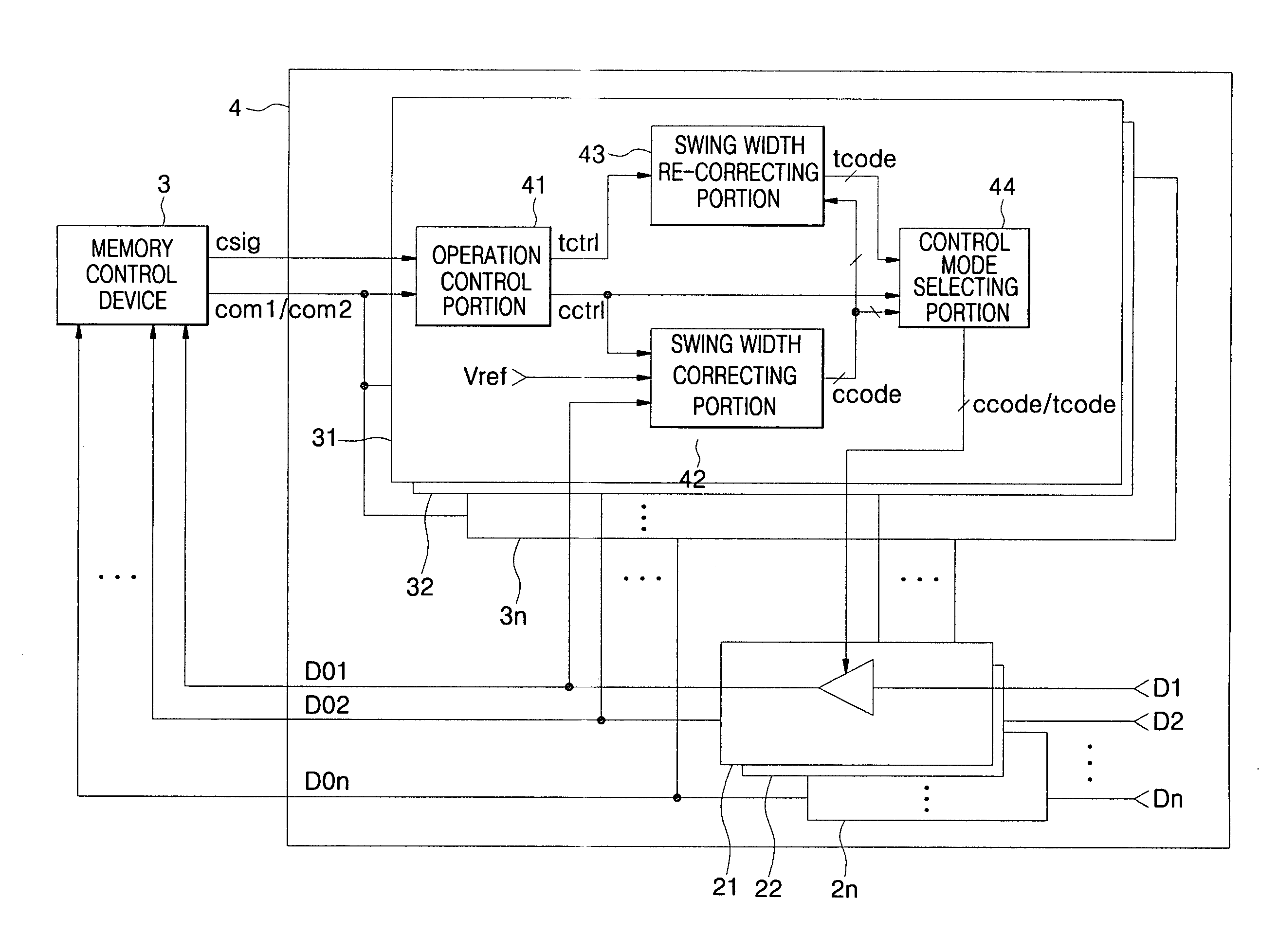
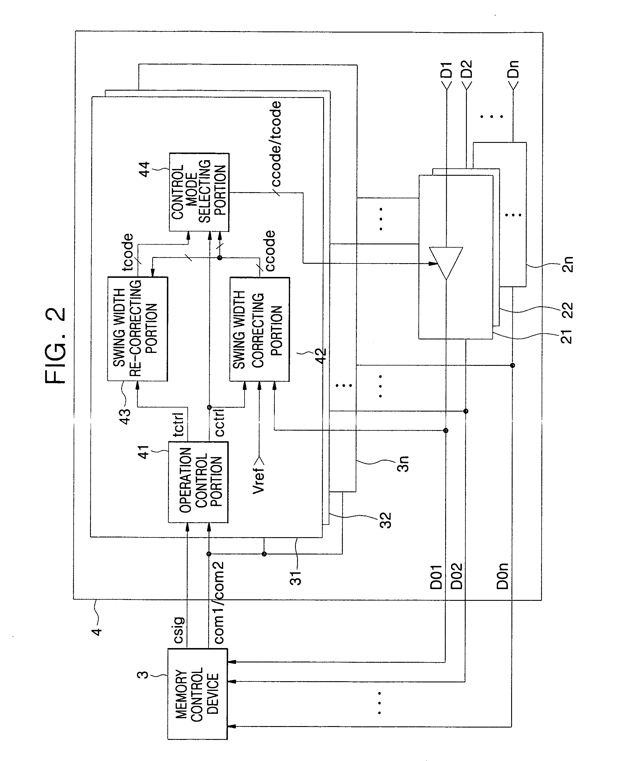
[0025] Example embodiments of the present invention provide a semiconductor memory device, a memory system having the same and a swing width control method thereof which considers the operation environment of the semiconductor memory device and the memory system to vary the data swing width of the semiconductor memory device, thereby reducing the power consumption and improving the operation performance of the memory system.

Problems solved by technology

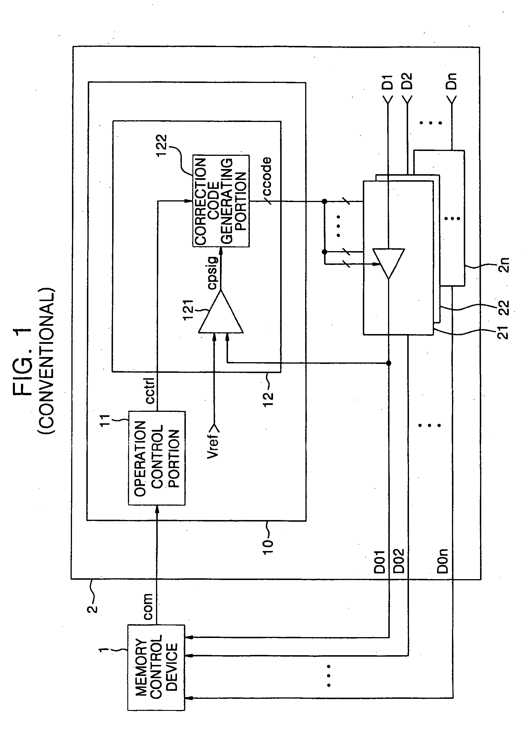
However, the correction swing width is generally directed towards satisfying the worst possible operation condition of the semiconductor memory device and thus, there is a problem because the data swing width may be excessively increased under a normal operation condition.
That is, the conventional data swing width controller may excessively increase the data swing widths of the plurality of output drivers 21 to 2n without considering the operation environment of the semiconductor memory device and the memory system, thereby increasing power consumption of the conventional semiconductor memory device.
Further, if data D01 to D0n output through the plurality of output drivers 21 to 2n are transmitted in the same direction, a simultaneous switching noise (SSN) phenomenon may occur due to the excessively increased data swing width and thus, the whole operation performance of the memory system may deteriorate.
The SSN represents a noise which may occur when a plurality of data is transmitted in the same direction through adjacent signal lines and an electric current of data flows excessively.
That is, a problem may occur in the conventional semiconductor device because the entire performance of the memory system depends on the data swing width of the reference output driver 21.

Method used


Image

  • Semiconductor memory device, memory system having the same, and swing width control method thereof
  • Semiconductor memory device, memory system having the same, and swing width control method thereof
  • Semiconductor memory device, memory system having the same, and swing width control method thereof

Examples


Embodiment Construction

[0048] Detailed illustrative embodiments of the present invention are disclosed herein. However, specific structural and functional details disclosed herein are merely representative for purposes of describing example embodiments of the present invention. This invention may, however, be embodied in many alternate forms and should not be construed as limited to only the embodiments set forth herein.

[0049] It will be understood that, although the terms first, second, etc. may be used herein to describe various components, these components should not be limited by these terms. These terms are only used to distinguish one component from another. For example, a first component could be termed a second component, and, similarly, a second component could be termed a first component, without departing from the scope of the present invention. As used herein, the term “and / or” includes any and all combinations of one or more of the associated listed items.

[0050] It will also be understood t...


PUM


Abstract

A semiconductor memory device that may include output drivers, each of which varies a data swing width in response to a correction code, and one or more data swing width control portions. Each of the data swing width control portions may correspond to an output driver, may vary the correction code according to a data swing width of the corresponding output driver to change the data swing width to a correction swing width, and then varies the correction code again to the extent that data of the corresponding output driver are normally transmitted, which may reduce the data swing width.

Description

PRIORITY STATEMENT [0001] This application claims the benefit of priority to Korean Patent Application No. 2006-0000641, filed Jan. 3, 2006, the entire contents of which are incorporated herein by reference. BACKGROUND OF THE INVENTION [0002] 1. Field of the Invention [0003] Example embodiments of the present invention relate to a semiconductor memory device and, more particularly, to a semiconductor memory device which can control a data swing width of an output buffer, a memory system having the same, and a swing width control method thereof. [0004] 2. Description of the Related Art [0005] A semiconductor memory device such as a DRAM, for example, should have a definite swing width of data transmitted through a wire line on a PCB substrate on which the semiconductor memory device may be mounted. For example, if a semiconductor memory device is mounted on a memory module, for example, a single in-line memory module (SIMM) or a double in-line memory module (DIMM), the swing width of...

Claims


Application Information

Patent Timeline
IPC IPC(8): G11C7/00
CPCG11C7/1051G11C2207/2254G11C11/4093G11C7/1069E03D9/08B05B12/00
Inventor CHOI, JUNG-HWAN
Owner SAMSUNG ELECTRONICS CO LTD
Learn More