Display device having a substrate with a polygonal display area and an electronic apparatus

a display device and display area technology, applied in the direction of semiconductor devices, electrical devices, organic semiconductor devices, etc., can solve the problems of display quality deterioration display quality deterioration, etc., and achieve high-quality display and suppress unnecessary display.

Active Publication Date: 2018-05-15
LUMITEK DISPLAY TECH LTD
View PDF26 Cites 0 Cited by
  • Summary
  • Abstract
  • Description
  • Claims
  • Application Information

AI Technical Summary

Benefits of technology

[0036]When the light, which is emitted from the light emitting elements, is reflected in the second surface of the transparent substrate and faces the direction of the element substrate, is incident to the display area and is reflected in the display area of the element substrate, there is a problem in that a display quality is deteriorated. When the thickness L1 of the transparent substrate satisfies the above-described Expression (1), the light, which is emitted from the light emitting elements, is reflected in the second surface of the transparent substrate and faces the direction of the element substrate, is incident to the periphery (non-display area) of the display area and is reflected in the non-display area of the element substrate, it is possible to suppress the display quality from being deteriorated.
[0039]When the light, which is emitted from the light emitting elements, is reflected in the second surface of the transparent substrate and faces the direction of the element substrate, is incident to the display area and is reflected in the display area of the element substrate, there is a problem in that a display quality is deteriorated. When the thickness L1 of the transparent substrate satisfies the above-described Expression (1), the light, which is emitted from the light emitting elements, is reflected in the second surface of the transparent substrate and faces the direction of the element substrate, is incident to the periphery (non-display area) of the display area and is reflected in the non-display area of the element substrate, it is possible to suppress the display quality from being deteriorated.
[0058]In the display device according to the application example, unnecessary display (deterioration of a display quality) is suppressed, and thus it is possible to provide a high-quality display. Accordingly, the electronic apparatus which includes the display device according to the application example can provide a high-quality display. For example, it is possible to apply the display device according to the application example to electronic apparatus which includes a display unit such as a head mounted display, a head up display, the electronic view finder of a digital camera, a portable information terminal, or navigation.

Problems solved by technology

However, when the color filters are omitted from the organic EL device disclosed in JP-A-2012-38677, some of light emitted from the organic EL elements is reflected between the counter substrate and the reflection layer, and thus there is a problem in that display qualities are deteriorated.
When the light, which is emitted from the light emitting elements, is reflected in the second surface of the transparent substrate and faces the direction of the element substrate, is incident to the display area and is reflected in the display area of the element substrate, there is a problem in that a display quality is deteriorated.

Method used


Image

  • Display device having a substrate with a polygonal display area and an electronic apparatus
  • Display device having a substrate with a polygonal display area and an electronic apparatus
  • Display device having a substrate with a polygonal display area and an electronic apparatus

Examples


first embodiment

Outline of Organic El Device

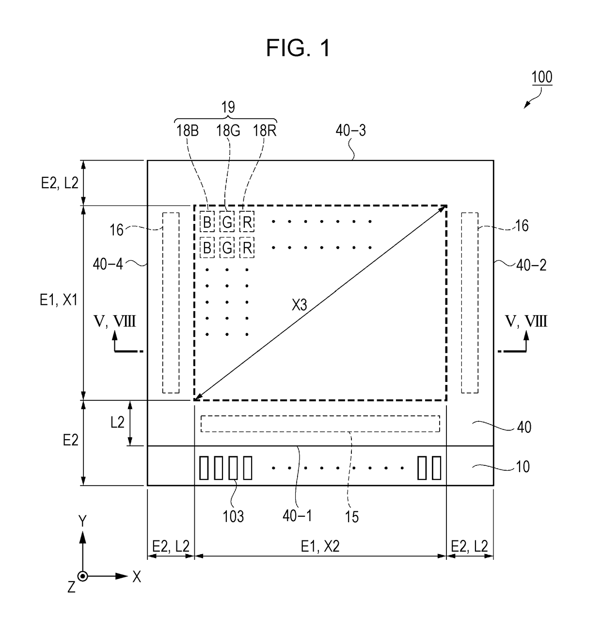
[0073]An organic EL device 100 according to a first embodiment is an example of a “display device” of the invention, and is a self-luminous micro display which is suitable for the display unit of a head mounted display which will be described later.

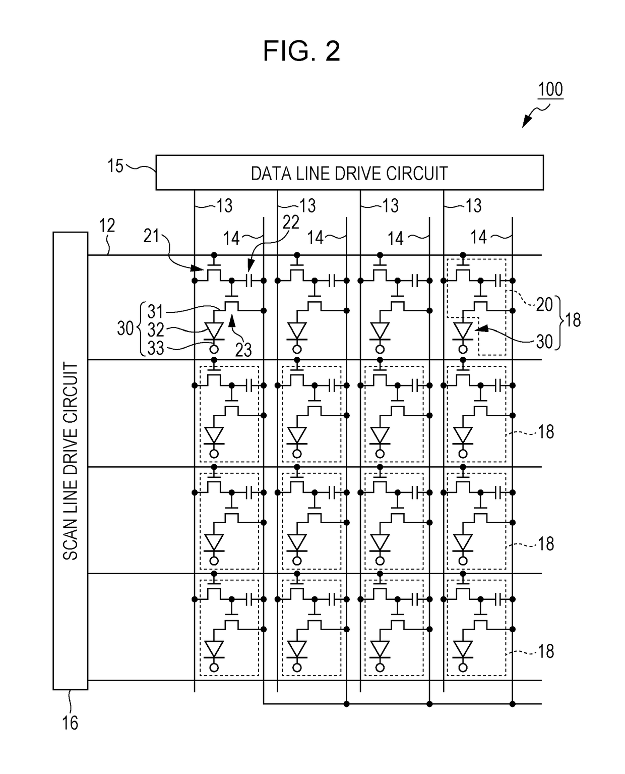
[0074]FIG. 1 is a schematic plan diagram illustrating the outline of an organic EL device according to the embodiment. FIG. 2 is an equivalent circuit diagram illustrating the electrical configuration of the organic EL device according to the embodiment.

[0075]First, the outline of the organic EL device 100 according to the embodiment will be described with reference to FIGS. 1 and 2.

[0076]As shown in FIG. 1, the organic EL device 100 according to the embodiment includes an element substrate 10 and a counter substrate 40 which is arranged to be face the element substrate 10. Both the substrates are bonded by a resin layer 42 (refer to FIG. 4) which will be described later.

[0077]The element substrate 10 includes ...

second embodiment

Electronic Apparatus

[0202]FIG. 9 is a schematic diagram illustrating a head mounted display as an example of electronic apparatus.

[0203]As shown in FIG. 9, a head mounted display 1000 includes two display units 1001 which are provided to correspond to right and left eyes. An observer M can watch letters, images and the like which are displayed on the display units 1001 by mounting the head mounted display 1000 like glasses on the head area. For example, when images are displayed on the right and left display units 1001 while taking parallax into consideration, it is possible to watch and enjoy stereoscopic images.

[0204]The organic EL device 100 according to the embodiment is mounted on the display units 1001. In the organic EL device 100, unnecessary display due to the reflection of light in the reflection layer 25 and the side surfaces 40-1, 40-2, 40-3, and 40-4 is suppressed, and thus it is possible to provide a high-quality display. Accordingly, when the organic EL device 100 acc...

first modification example

[0208]FIG. 10 is a diagram corresponding to FIG. 5 and is a schematic cross-sectional diagram illustrating the configuration of an organic EL device according to a first modification example. In the organic EL device 200 according to the modification example, the light shielding layer 51 of the organic EL device 100 according to the first embodiment is omitted, and a resin layer (second resin layer 42b), which absorbs light in at least one position of the non-display area E2, is newly arranged. This is the difference between the modification example and the first embodiment.

[0209]As shown in FIG. 10, a resin layer 42, which is arranged between the element substrate 10 and the counter substrate 40, includes a first resin layer 42a which has transparency and a second resin layer 42b which has a light shielding property. The first resin layer 42a is arranged in the display area E1 and the second resin layer 42b is arranged in at least a part of the non-display area E2. The second resin...


PUM


Abstract

There is provided a display device including an element substrate that has a display area; and a counter substrate. When it is assumed that the length of the shortest edge of the display area is X1, the length of a longest diagonal line of the display area is X3, the thickness of the counter substrate is L1, the refraction index of the counter substrate is n1, the refractive index of the air is n2, and the minimum value of an angle, which is generated between a progress direction of light emitted from the organic EL elements and a normal vector direction is totally reflected in the surface, is α, the relationship of X1 / (2 tan α)≤L1≤X3 / (tan α) is realized.

Description

BACKGROUND[0001]1. Technical Field[0002]The present invention relates to a self-luminous display device and an electronic apparatus including the display device.[0003]2. Related Art[0004]For example, an organic EL device in which pixels having transistors and organic electro-luminescence (hereinafter, referred to as an organic EL) elements are arranged in a matrix shape has been proposed as an example of a display device (JP-A-2012-38677).[0005]In the organic EL device disclosed in JP-A-2012-38677, a reflection layer, a reflection layer protection layer (insulation film), an organic EL element, a protection layer, a color filter, a light-transmitting counter substrate, and the like are laminated in order on a substrate on which transistors are formed. The organic EL element includes a pixel electrode, a light emitting function layer, and a cathode which are laminated in order from a side of the insulation film. The organic EL device has an optical resonance structure in which the op...

Claims


Application Information

Patent Timeline
Patent Type & Authority Patents(United States)
IPC IPC(8): H01L29/18H01L33/00H01L51/52
CPCH01L51/5271H01L51/524H01L51/5265H01L2251/558H01L51/5284H01L2251/5315H01L51/5275H10K50/852H10K50/841H10K50/856H10K50/858H10K50/865H10K2102/3026H10K2102/351
Inventor SHIRATORI, KOYAKOSHIHARA, TAKESHI
Owner LUMITEK DISPLAY TECH LTD
Why Eureka
Try Eureka