Small-aperture-ratio display with electrical component

a technology of electrical components and small aperture ratios, applied in the direction of identification means, instruments, semiconductor devices, etc., can solve the problems of reduced lifetime, especially low aperture ratio, and low aperture ratio, so as to improve functionality, increase lifetime and image quality, and reduce costs

Active Publication Date: 2018-06-05
X DISPLAY CO TECH LTD
View PDF330 Cites 28 Cited by
  • Summary
  • Abstract
  • Description
  • Claims
  • Application Information

AI Technical Summary

Benefits of technology

[0013]According to embodiments of the present invention, an inorganic light emitter such as an LED provides high-brightness light (for example having an efficiency or brightness greater than incandescent, fluorescent, or OLED light emitters) output without depending on a relatively large light-controlling area and without restrictions on viewing angle, thus providing increased lifetime and image quality. By printing light emitters formed in a crystalline semiconductor wafer onto a display substrate using conventional materials and processes, costs are reduced and functionality improved. Light-emitting diodes occupy relatively less area on a display substrate, providing space to construct or otherwise provide additional circuits and devices on the display substrate, increasing the functionality of the small-aperture-ratio device. Among other things, the small-aperture-ratio display provides increased lifetime, image quality, ease of manufacturing, and reduced cost and improved functionality in a simpler and more robust structure.

Problems solved by technology

Low aperture ratios are especially problematic for displays in which the light-controlling elements (e.g. light-transmissive or light-emitting elements) are located on the same substrate as the active control elements (such as thin-film transistors), for example a bottom-emitting OLED display in which the display substrate area is shared between the control circuits and the light-emitting area.
Active-matrix LC displays suffer from the same problem and, in addition, the active control elements are located between the light emitter (the backlight) and a viewer.
The increased brightness results in a reduced lifetime.

Method used


Image

  • Small-aperture-ratio display with electrical component
  • Small-aperture-ratio display with electrical component
  • Small-aperture-ratio display with electrical component

Examples


Embodiment Construction

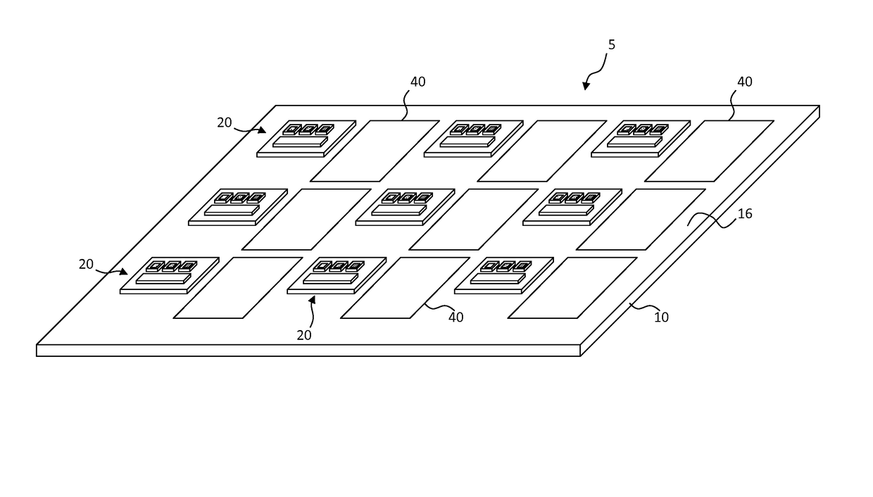
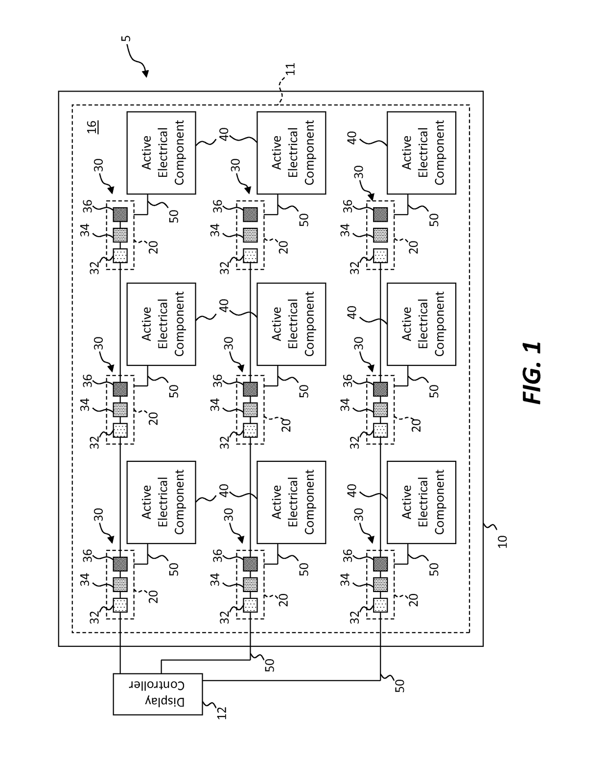
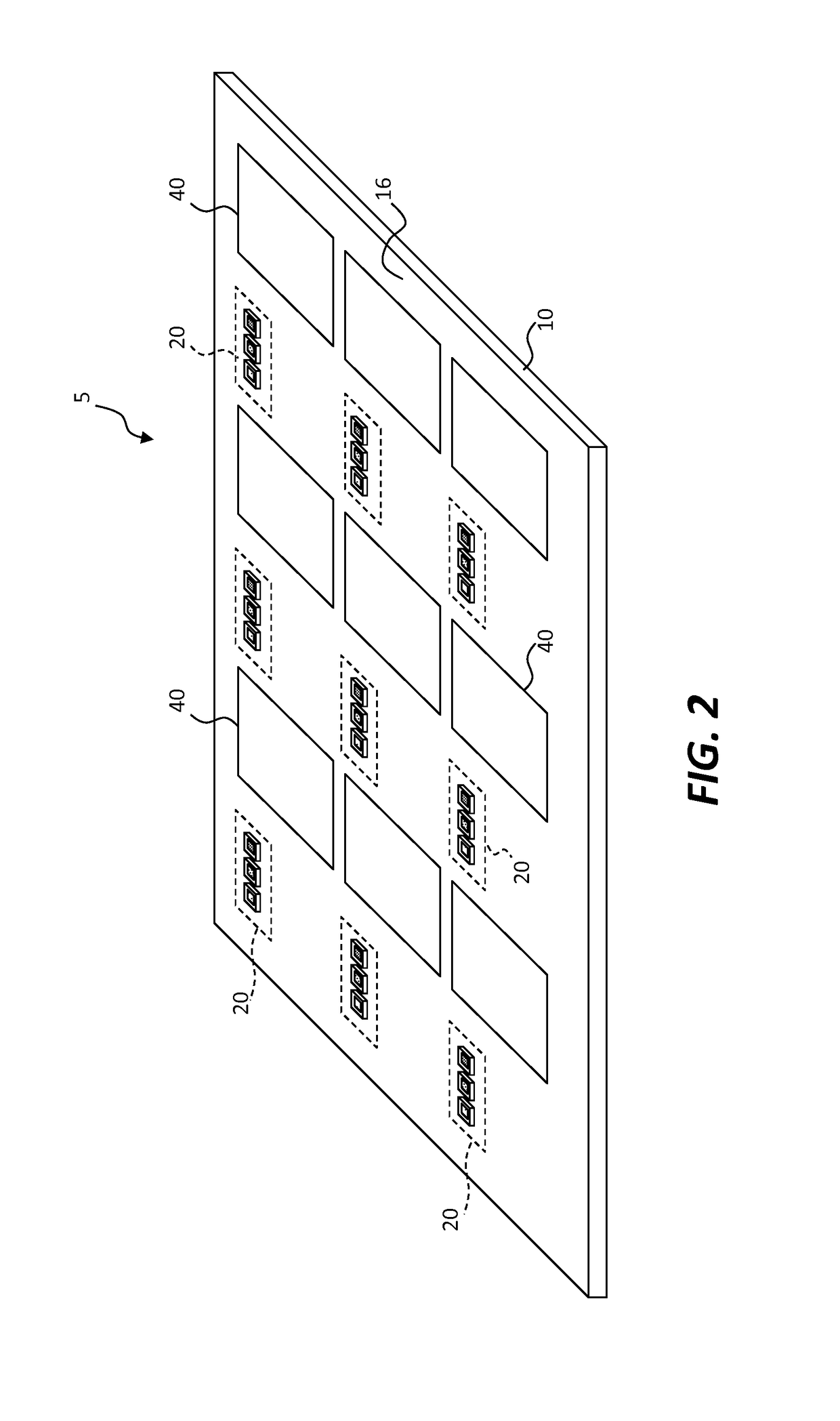
[0115]Referring to the plan view of FIG. 1 and the perspective of FIG. 2, in an embodiment of the present invention a small-aperture-ratio display 5 includes a display substrate 10. A plurality of spatially separated pixel elements 20 are distributed over the display substrate 10, each pixel element 20 including one or more light emitters 30. As illustrated in FIG. 1, the light emitters 30 include a red light emitter 32, a green light emitter 34, and a blue light emitter 36 in each pixel element 20. In some embodiments, additional light emitters are includes, such as a yellow light emitter. An active electrical component 40 is electrically connected to each of the pixel elements 20, each active electrical component 40 located on the display substrate surface 16 or in the display substrate 10 at least partly between the pixel elements 20.

[0116]The active electrical components 40 provide additional functionality to the small-aperture-ratio display 5 without compromising the image qual...


PUM


Abstract

A small-aperture-ratio display includes a display substrate and a plurality of spatially separated pixel elements distributed over the display substrate. Each pixel element includes one or more light emitters. An active electrical component is electrically connected to each of the pixel elements and each active electrical component is located on the display substrate at least partly between the pixel elements. The display substrate has a contiguous display substrate area that includes the pixel elements, the light emitters each have a light-emissive area, and the substrate area is greater than or equal to one-quarter the combined light-emissive areas of the light emitters.

Description

PRIORITY APPLICATION[0001]This application claims priority to and the benefit of U.S. Provisional Patent Application No. 62 / 164,953, filed May 21, 2015, titled “Small-Aperture-Ratio Display with Electrical Component,” the contents of which are incorporated by reference herein in its entirety.CROSS REFERENCE TO RELATED APPLICATIONS[0002]Reference is made to U.S. patent application Ser. No. 62 / 055,472 filed Sep. 25, 2014, entitled Compound Micro-Assembly Strategies and Devices, and to U.S. patent application Ser. No. 62 / 148,603 filed Apr. 16, 2015, entitled Micro-Assembled Micro LED Displays and Lighting Elements, the contents of each of which are incorporated by reference herein in their entirety.FIELD OF THE INVENTION[0003]The present invention relates to a display having a small aperture ratio and a display substrate with distributed light emitters.BACKGROUND OF THE INVENTION[0004]Flat-panel displays are widely used in conjunction with computing devices, in portable devices, and fo...

Claims


Application Information

Patent Timeline
Patent Type & Authority Patents(United States)
IPC IPC(8): H01L21/77G09F9/33
CPCG09F9/33H01L21/77H01L25/0753H01L25/167
Inventor BOWER, CHRISTOPHERROTZOLL, ROBERT R.MEITL, MATTHEWCOK, RONALD S.
Owner X DISPLAY CO TECH LTD
Why Eureka
Try Eureka