Interposer and electrical testing method thereof

a technology of interposers and electrical testing methods, applied in the direction of individual semiconductor device testing, semiconductor/solid-state device testing/measurement, instruments, etc., can solve the problem that the wafer testing method cannot be used to detect the electrical performance of the interposer, and achieve the effect of effective electrical testing

Active Publication Date: 2018-06-05
SILICONWARE PRECISION IND CO LTD
View PDF4 Cites 2 Cited by
  • Summary
  • Abstract
  • Description
  • Claims
  • Application Information

AI Technical Summary

Benefits of technology

[0010]According to the present invention, by forming a removable electrical connection structure on a surface of the interposer for electrically connecting a plurality of conductive pads on the surface, the conductive through holes in the interposer, the conductive pads on opposite surfaces of the interposer and the removable electrical connection structure form a circuit for electrical testing, the electrical performance of the conductive through holes. Thereafter, the removable electrical connection structure is removed without adversely affecting the interposer. Therefore, the present invention provides an effective electrical testing method of the interposer without adversely affecting the original design of the interposer.

Problems solved by technology

Further, since the upper and lower surfaces of the interposer 10 have external conductive elements disposed thereon, a conventional wafer testing method cannot be used to detect the electrical performance of the interposer 10.

Method used


Image

  • Interposer and electrical testing method thereof
  • Interposer and electrical testing method thereof
  • Interposer and electrical testing method thereof

Examples


first embodiment

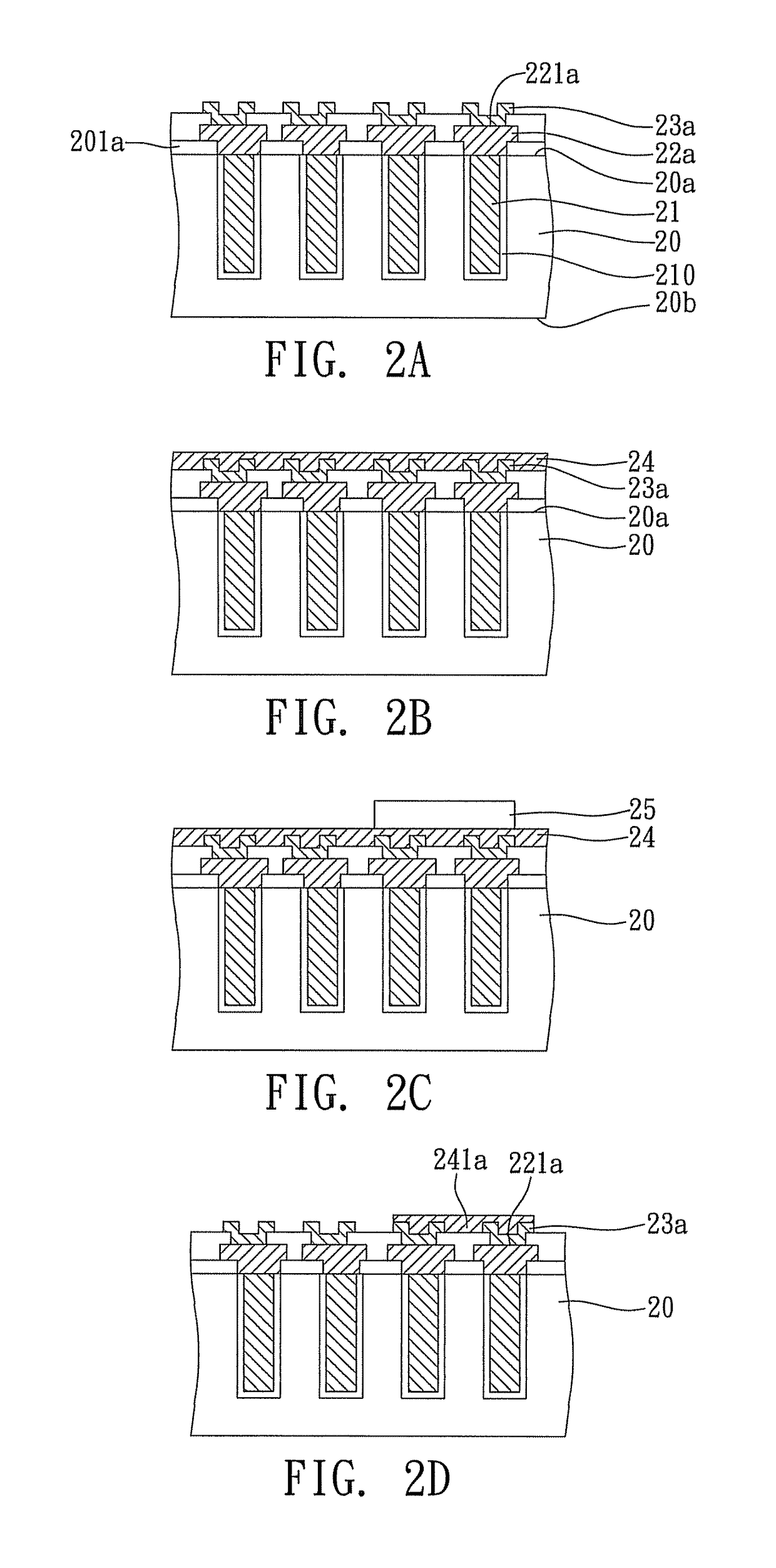
[0020]FIGS. 2A to 2K are cross-sectional views showing an electrical testing method of an interposer according to the present invention. FIG. 2H′ shows another embodiment of FIG. 2H.

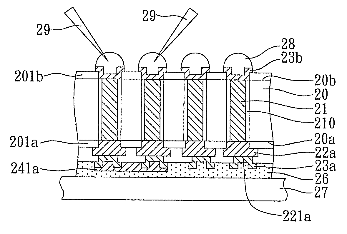
[0021]Referring to FIG. 2A, an interposer is provided. The interposer has a substrate 20 having opposite first and second surfaces 20a, 20b and a plurality of conductive through holes 21 formed therein. The first surface 20a of the substrate 20 has at least a first redistribution layer (RDL) 22a. The outermost first redistribution layer 22a has a plurality of first conductive pads 221a electrically connected to the conductive through holes 21, and a UBM (Under Bump Metallurgy) layer 23a is further formed on the first conductive pads 221a. An insulating layer 210 made of SiO2 or SiN is formed between the substrate 20 and each of the conductive through holes 21. The substrate 20 can be made of silicon or glass, and have a thickness less than or equal to 200 um, preferably less than 100 um. In addition, a f...

third embodiment

[0032]FIG. 4 shows an electrical testing method of an interposer according to the present invention. The first surface 20a of the substrate 20 further has at least a testing pad 2211 electrically connected to one of the first conductive pads 221a through a circuit 2411a. Alternatively, the testing pad 2211 can be disposed on the second surface 20b. To perform an electrical test, a probe 29 can be connected to the testing pad 2211 instead of the corresponding first conductive pad 221a, thereby protecting the surface of the first conductive pad 221a from being damaged by the probe 29 so as to ensure the product reliability.

fourth embodiment

[0033]FIGS. 5A and 5B are schematic cross-sectional and top views of an electrical testing method of an interposer according to the present invention.

[0034]The fourth embodiment differs from the second embodiment in that a second removable electrical connection structure 241b is formed on the second surface 20b and electrically connected to a portion of the second UBM layer 23b. The first and second conductive pads 221a, 221b, the first and second removable electrical connection structures 241a, 241b, and the conductive through holes 21 form a daisy chain structure. By measuring the impedance of the daisy chain structure, the present invention can determine whether the interposer has defective conductive through holes that lead to increase of the impedance value.

[0035]FIG. 6 shows an electrical testing method of an interposer according to a fifth embodiment of the present invention. The fifth embodiment differs from the fourth embodiment in that two probes 29′ are connected in serie...


PUM


Abstract

An interposer is provided which includes: a substrate having a first surface with a plurality of first conductive pads and a second surface opposite to the first surface, the second surface having a plurality of second conductive pads; a plurality of conductive through holes penetrating the first and second surfaces of the substrate and electrically connecting the first and second conductive pads; and a first removable electrical connection structure formed on the first surface and electrically connecting a portion of the first conductive pads so as to facilitate electrical testing of the interposer.

Description

CROSS-REFERENCES TO RELATED APPLICATIONS[0001]This application claims under 35 U.S.C. § 119(a) the benefit of Taiwanese Application No. 101109806, filed Mar. 22, 2012, the entire contents of which is incorporated herein by reference.BACKGROUND OF THE INVENTION[0002]1. Field of the Invention[0003]The present invention relates to interposers and electrical testing methods thereof, and, more particularly, to an interposer having a plurality of conductive through holes and an electrical testing method thereof.[0004]2. Description of Related Art[0005]FIG. 1 shows a cross-sectional view of a conventional 3D-IC package structure. Referring to FIG. 1, an interposer 10 having a plurality of copper posts 11 penetrating therethrough is disposed between a semiconductor chip 12 and a packaging substrate 13 to serve as an electrical connection bridge between the semiconductor chip 12 and the packaging substrate 13.[0006]The copper posts 11 are formed by filling a copper material in a plurality of...

Claims


Application Information

Patent Timeline
Patent Type & Authority Patents(United States)
IPC IPC(8): H01L21/66H01L23/498H01L21/48
CPCH01L22/14H01L21/486H01L22/20H01L23/49822H01L23/49827H01L23/49816H01L2224/16
Inventor CHEN, LU-YICHIU, CHI-HSINCHIU, SHIH-KUANG
Owner SILICONWARE PRECISION IND CO LTD
Why Eureka
Try Eureka