Multicore processor test method

a multi-core processor and test method technology, applied in the direction of unauthorized memory use protection, memory adressing/allocation/relocation, instruments, etc., can solve the problem of limiting the performance improvement that could be achieved on a single computer system, increasing control complexity, and complex server hardware becomes a problem, so as to achieve the effect of lsi tests more efficiently

Active Publication Date: 2008-04-01
FUJITSU LTD
View PDF4 Cites 39 Cited by
  • Summary
  • Abstract
  • Description
  • Claims
  • Application Information

AI Technical Summary

Benefits of technology

[0034]The present invention advantageously simplifies and accelerates identification of not only completely defect-free LSIs but also partially defect-free LSIs, and improves yield and reduces costs by salvaging partially core defect-free LSIs during semiconductor manufacture, which is to be achieved in that, in order to more efficiently identify completely defect-free LSI / partially defect-free LSI / defective LSI in an LSI test for processors having a multicore, such as CMPs, out of the LFSR (Linear Feedback Shift Register) based test pattern generating circuit and the MISR (Multiple Input Signature Register) based test pattern compression circuit which make up logic BIST circuits that are installed in processors, a MISR test pattern compression circuit that performs test pattern compression in the LSI test is to be provided independently for each core block and for the CMP common block.
[0052]According to the present invention, as described above, providing an independent MISR test pattern compression circuit for each logic block in a multicore processor such as a CMP comprising a plurality of processor cores makes it possible to perform LSI tests more efficiently.

Problems solved by technology

However, with loose coupling using a cluster configuration, communication overhead between the server nodes becomes a problem, while in the case of close coupling using SMP, complexity of the server hardware becomes a problem, and in both cases, with conventional architecture, there is a limit to the performance improvement that could be achieved on a single computer system.
However, in the case of multicore configurations such as CMP, contrary to the improvements in processing performance achieved by increasing the number of cores, there are problems such as increasing complexity of control due to installation of a plurality of cores and lower yields during semiconductor manufacturing due to increased die size.
The reduced yields during semiconductor manufacturing due to the increased die size are a particularly important problem for multicore processors such as CMPs comprising a multicore.
However, with the increasing scale of LSI logic, such as processors manufactured to a high scale of integration by recent ultramicro processes, it has become impossible to disregard the scale of the test pattern size.
Increased test pattern size not only affects production efficiency by requiring a longer time for LSI component testing, but also requires more advanced and high performance LSI testers, leading to increased costs of LSI testing.
Furthermore, even assuming it were possible to analyze the test results for each individual logic block based on said single signature, there was still the problem that identification of a defect-free LSI is not possible unless the comparison of all the logic blocks against the expected value data is completed.
Namely, for multicore processors comprising a plurality of cores, there was the problem that the testing costs for completely defect-free LSI test result analysis were the same as for partial core defect-free test result analysis.
In the prior art, as described above, in a processor with a multicore configuration based on CMP or the like, reduced yield due to increased die size was a problem.
However, in the prior art, identifying a partially defect-free LSI at the time of manufacturing required collection and analysis of scan data for all scan points, etc., just as for completely defect-free LSIs, so the analysis was complicated and the LSI test was costly and time-consuming.

Method used


Image

  • Multicore processor test method
  • Multicore processor test method
  • Multicore processor test method

Examples


Embodiment Construction

[0068]A first through sixth modes of embodiment of the present invention are described in detail below with reference to the drawings.

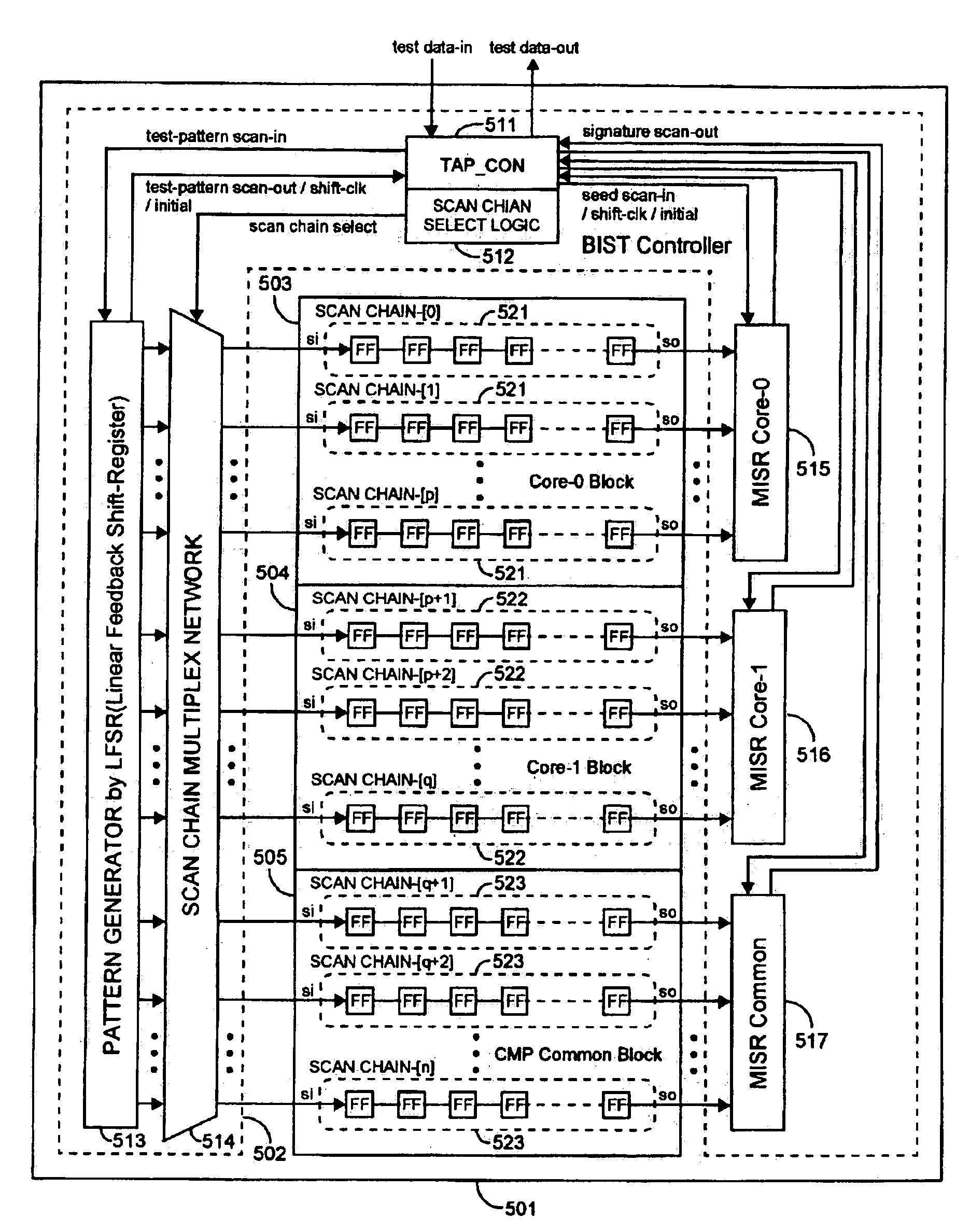
[0069]FIG. 5 is a drawing illustrating a first mode of embodiment of the present invention for a 2-CMP multicore processor comprising two core blocks.

[0070]Processor 501 is a 2-CMP multicore processor comprising a logic BIST circuit block 502, core-0 block 503, core-1 block 504, and CMP common block 505. Furthermore, the logic BIST circuit block 502 contains a TAP controller 511, scan chain selection control circuit 512, LFSR test pattern generating circuit 513, scan chain switching MUX circuit 514, core-0 block MISR test pattern compression circuit 515, core-1 block MISR test pattern compression circuit 516, and CMP common block MISR test pattern compression circuit 517.

[0071]First, the scan chain selection control circuit 412 is controlled by the TAP controller 511 and the scan chain is switched by the scan chain switching MUX circuit 514 from syste...


PUM


Abstract

In processors having multiple cores, such as CMPs, an independent MISR test pattern compression circuit is provided for each logic block, which makes it possible to perform LSI tests more efficiently. A processor includes a plurality of logic block circuits, which include at least a first processor core circuit and a second processor core circuit, each processor core circuit having a scan chain circuit and being operable independently, and a common block circuit having a scan chain circuit and a cache circuit that is shared by the first processor core circuits and the second processor core circuits. The processor further includes, for each logic block, a test pattern generating circuit operable to generate a test pattern and input the test pattern to the scan chain of each logic block circuit, and a test pattern compression circuit operable to accept as input and compress the test pattern output by the scan chain of each logic block circuit.

Description

CROSS REFERENCE TO RELATED APPLICATION[0001]This application is related to and claims priority to Japanese Application No. 2004-127216 filed Apr. 22, 2004 in the Japanese Patent Office, the contents of which are incorporated by reference herein.BACKGROUND OF THE INVENTION[0002]1. Field of the Invention[0003]The present invention relates to processors such as a CPU (Central Processing Unit), MPU (Micro Processing Unit), DSP (Digital Signal Processor) or GPU (Graphics Processing Unit: graphics processor, or image processing LSI or geometry engine), comprising a plurality of execution units (hereinafter referred to simply as “cores”), and to testing methods for such processors.[0004]2. Description of the Related Art[0005]Conventionally, in computer systems, such as servers, where especially high processing capacity is required, such as for the primary business processing of an enterprise, improvements in processing capacity have been achieved by connecting a plurality of processors via...

Claims


Application Information

Patent Timeline
Patent Type & Authority Patents(United States)
IPC IPC(8): G01R31/28G01R31/3185G06F9/26G06F9/34G06F11/00G06F11/22G06F11/263G06F11/267G06F12/00G06F12/02G06F12/04G06F12/08G06F12/10G06F12/14G06F12/16G06F13/00G06F13/28H01L21/822H01L27/04
CPCG01R31/318547G06F11/263G06F11/267
Inventor OHWADA, AKIHIKONAKADA, TATSUMIYAMANAKA, HITOSHI
Owner FUJITSU LTD
Why Eureka
Try Eureka