Unlock instant, AI-driven research and patent intelligence for your innovation.

Method of replacing special hardware interface for NAND type flash memory

A special hardware and flash memory technology, which is applied in the field of NAND flash memory devices, can solve problems such as complex operation interface and increased cost of using NAND flash memory, and achieve the effects of improving execution efficiency, reducing production costs, and saving CPU resources

Inactive Publication Date: 2008-02-13
INVENTEC APPLIANCES (SHANGHAI) CO LTD
View PDF3 Cites 0 Cited by
  • Summary
  • Abstract
  • Description
  • Claims
  • Application Information

AI Technical Summary

Problems solved by technology

However, although the NAND flash memory chip has a small area and high capacity, its operation interface is much more complicated than that of the NOR flash memory, and it needs a dedicated hardware interface to manage and operate it, which invisibly increases the cost of using the NAND flash memory

Method used


Image

  • Method of replacing special hardware interface for NAND type flash memory

Examples


Embodiment Construction

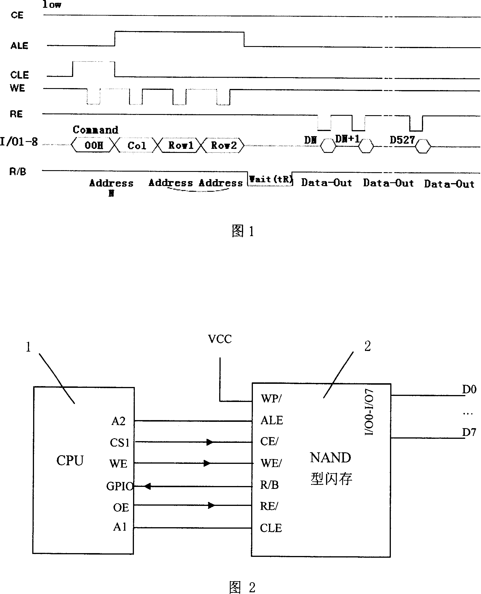
[0024] As shown in Figure 2, connect the address lines A1 and A2 of the CPU to the CLE and ALE pins of the NAND flash memory respectively; connect the WE and OE pins of the CPU to the WE and RE pins of the NAND flash memory respectively; GPIO function pin and NAND flash memory R / B pin; CS1 pin of CPU can be used, and CS of other CPU can also be selected X pins, such as CS 1 -CX 7 , connect the CE pin of the NAND flash memory.

[0025] Since the operating program of the NAND flash memory of the present invention is above the operating system (OS), the memory management unit (MMU) has shielded the direct access of the program to the underlying hardware at this time, so the MMU needs to be set to open up an NAND flash memory. A memory (Memory) image area, so that our code can operate on it. In the connection mode shown in Figure 2, use the CS1 pin of the CPU to control the CE signal of the NAND-Flash. If CS1 is mapped to the address 0x24000000, then reading and writing the add...


PUM


Abstract

The invention discloses a method for replacing the dedicate hardware interface of NAND flash memory. The NAND flash memory supports CD don't care operation mode, which connects six lead terminals of CPU with NAND flash memory lead terminals CLE, ALE, WE, RE, CE, R / B respectively; setting image address for the CPU lead terminal connected with the CE terminal of the NAND flash memory; setting input mode for the CPU terminal connected with the R / B terminal of the NAND flash memory; identifying flash memory operation address according to the CPU terminals connected with the CLE, ALE and CE terminal of the NAND flash memory.

Description

technical field [0001] The present invention relates to a method for using a NAND flash memory device, in particular to a method for using software programming and CPU pins to replace the dedicated hardware interface of the NAND flash memory on mobile handheld devices such as PDAs. technical background [0002] NOR and NAND are the two main non-volatile flash memory (flash) technologies currently on the market. Due to the large capacity of NAND flash memory, the price per unit capacity is low, and the speed is much higher than that of NOR flash memory (NOR-Flash). On mobile devices The use of NAND flash memory can greatly improve the cost performance of mobile flash memory storage. However, although the NAND flash memory chip has a small area and high capacity, its operation interface is much more complicated than that of the NOR flash memory, and requires a dedicated hardware interface to manage and operate it, which virtually increases the cost of using the NAND flash memo...

Claims


Application Information

Patent Timeline
Patent Type & Authority Patents(China)
IPC IPC(8): G06F13/00
Inventor 李赟何代水
Owner INVENTEC APPLIANCES (SHANGHAI) CO LTD