
Method for recognizing work in die bonder and die bonder

A technology of attachment device and identification method, which is applied in the direction of electrical components, electric solid devices, semiconductor devices, etc., can solve the problems of high price, long time, and high price of chip attachment devices, and achieve the elimination of useless bonding time, increase productivity, and reduce costs Effect

Inactive Publication Date: 2008-04-23
CANON MACHINERY
View PDF4 Cites 0 Cited by
  • Summary
  • Abstract
  • Description
  • Claims
  • Application Information

AI Technical Summary

Problems solved by technology

[0007] However, for example, in the chip attaching device shown in FIG. 15, if a CCD camera is used as the first and second image recognition devices 180 and 190, the CCD camera has a low resolution of about 300,000 pixels, so for example All bonding regions 151 of each row in the width direction on substrates 150 such as lead frames and printed wiring boards cannot simultaneously perform image recognition with high precision, and as shown in FIG. Figure 16 As shown, image recognition is repeatedly performed on only a part of the bonding regions 151 in all the bonding regions 151 of each column, and when the processing based on the image recognition is completed, the CCD cameras 180 and 190 are moved along the direction of the substrate 150 as shown in the figure. Move in the width direction, perform image recognition on other joining regions 151 in the column, and perform processing actions based on the image recognition
[0008] Therefore, the moving mechanism that makes the supporting member of CCD camera 180,190 move along the width direction of substrate 150 is indispensable, not only make the supporting mechanism of camera complicate and enlarge, and become expensive, also because CCD camera 180, 190 to the width direction of the movement time, and because it is necessary to wait for image recognition until the image shaking caused by the vibration caused by the movement of the support member subsides, image recognition and processing take a long time, and there is a problem that it is impossible to make the chip The problem of increasing the speed of the attachment device
Or, in order to prevent vibration, an anti-vibration mechanism is required, and there is also a problem that the chip attaching device becomes expensive
[0009] In addition, since it is necessary to estimate the timing at which the imaging field of view is not blocked by the mechanism that reciprocates over the imaging area, and ensure the imaging timing, there is also a problem that the speed of the die attaching device cannot be increased.

Method used


Image

  • Method for recognizing work in die bonder and die bonder
  • Method for recognizing work in die bonder and die bonder
  • Method for recognizing work in die bonder and die bonder

Examples


Embodiment Construction

[0113] Next, an embodiment of a die attach apparatus employing the workpiece recognition method of the present invention will be described with reference to the drawings.

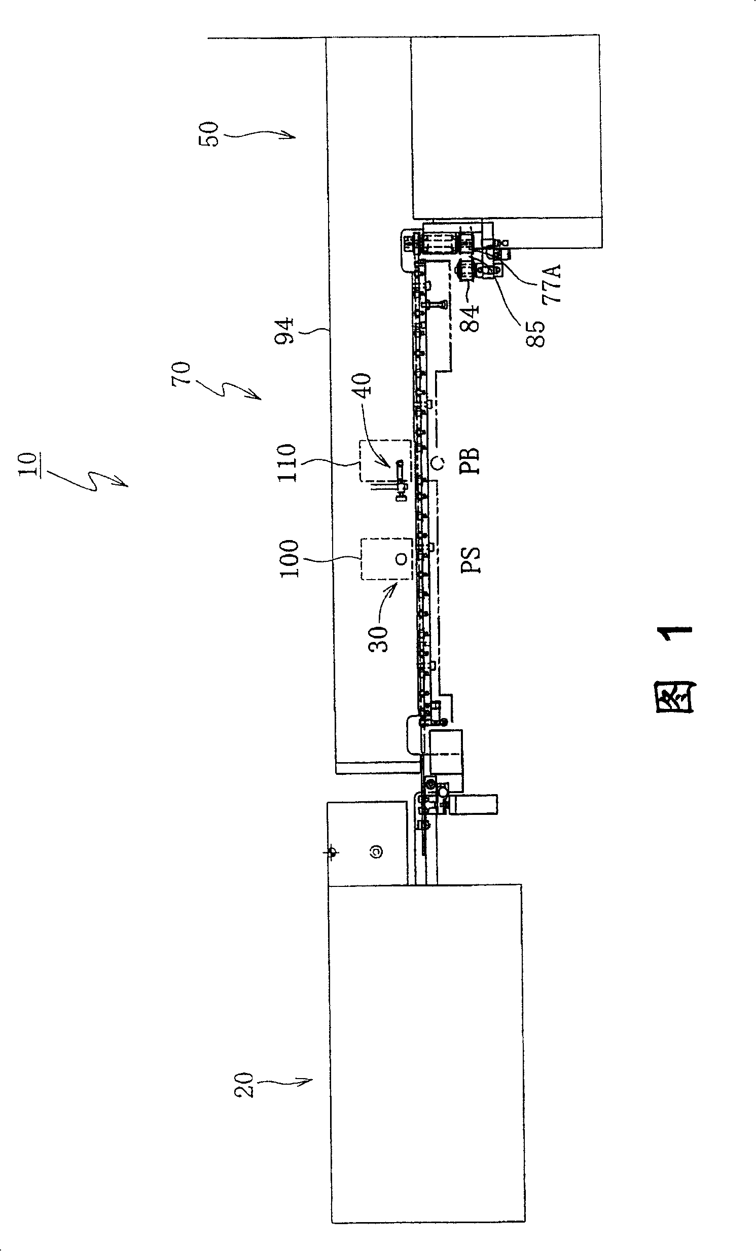
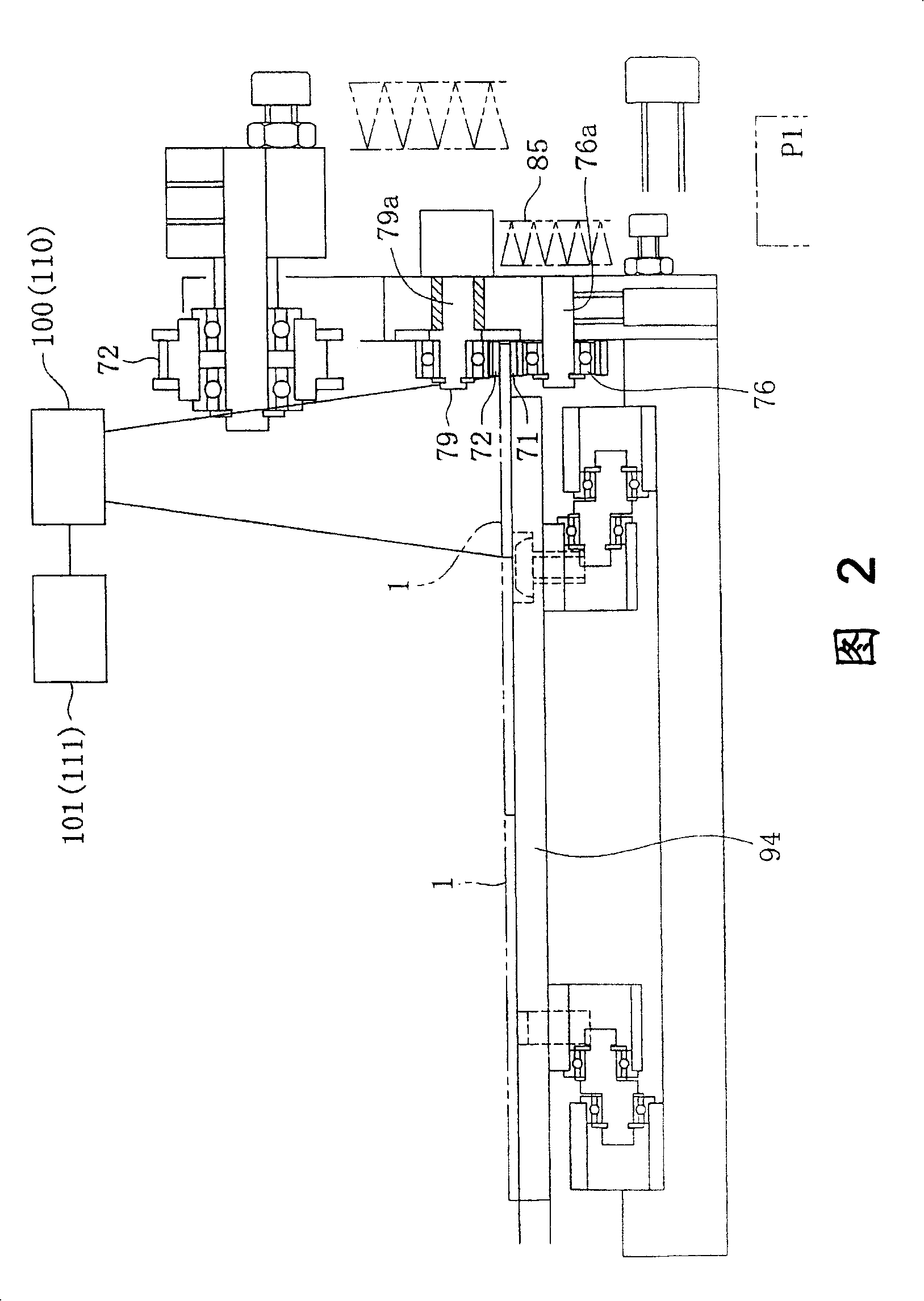
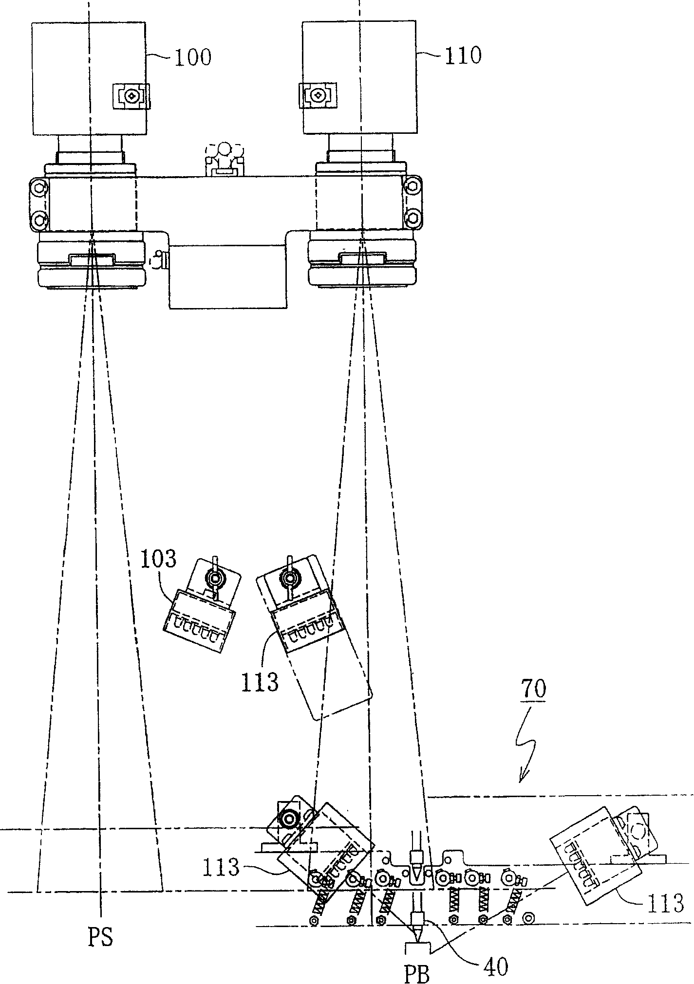
[0114] The chip attaching device 10 is shown in Fig. 1- image 3 As shown, it includes: a loader 20 for supplying a substrate 1 having a plurality of bonding regions such as a lead frame and a printed circuit board as an example of a workpiece, a transport device 70 for transporting the substrate 1 , and a transport device 70 in the transport device 70. The bonding material coating position PB on the front side of the halfway portion of the substrate 1 applies the bonding material to the bonding material coating device 30 on the substrate 1, and the bonding material coating position PB on the front side of the midway portion of the transport device 70 applies the bonding material to the substrate 1. Bonding head 40 (bonding head) for bonding semiconductor chip (chip) (die) on substrate 1 of bonding material...


PUM


Abstract

In order to perform image recognition at higher speed and with higher accuracy in a die bonder, a first high-function camera (100) is disposed fixedly above a position coated with bonding material (ps) located on this side in the middle of carrying passage of a carrier (70) and a second high function camera (110) is disposed fixedly above the bonding position (pb) of a semiconductor chip located on the forward side in the middle of carrying passage of the carrier (70). The first high function camera (100) image-recognizes the coating state of bonding material for all bonding regions (2) collectively at least in one row in the widthwise direction of a substrate, and the second high function camera (110) image-recognizes the bonding state of the semiconductor chip for all bonding regions (2) collectively at least in one row in the widthwise direction of the substrate (1).

Description

technical field [0001] The present invention relates to a workpiece identification method in a chip attaching device and a chip attaching device using the method, for example, relates to a method for applying a bonding material on a substrate suitable for having multiple bonding regions (islands), and A method for recognizing a workpiece in a die attach device of a die attach device for bonding semiconductor chips, and a die attach device. Background technique [0002] Semiconductor devices generally bond the back of a semiconductor chip (die) to a substrate such as a lead frame and a printed circuit board through a bonding material such as solder, hard solder, silver paste, or resin. while manufacturing. [0003] In such a die attach apparatus for bonding a semiconductor chip (chip) to a substrate, as shown in FIG. 15(A) and FIG. The substrate 150 is supplied one by one from the loader 120 to the conveying device 130, and the substrate 150 is conveyed in a set direction o...

Claims


Application Information

Patent Timeline
Patent Type & Authority Patents(China)
IPC IPC(8): H01L21/52G06T7/00
CPCH01L21/6836H01L2221/68327G06T7/0004H01L2924/19041H01L2924/3025H01L2221/68336
Inventor 三木耕司光藤淳
Owner CANON MACHINERY
Learn More