Display
A technology of display devices and light-emitting layers, applied in lighting devices, static indicators, instruments, etc., can solve problems such as intermittent animation display, and achieve the effects of eliminating uneven brightness, reducing electrical power loss, and reducing power loss.
- Summary
- Abstract
- Description
- Claims
- Application Information
AI Technical Summary
Problems solved by technology
Method used
Image

Examples
no. 1 approach 》
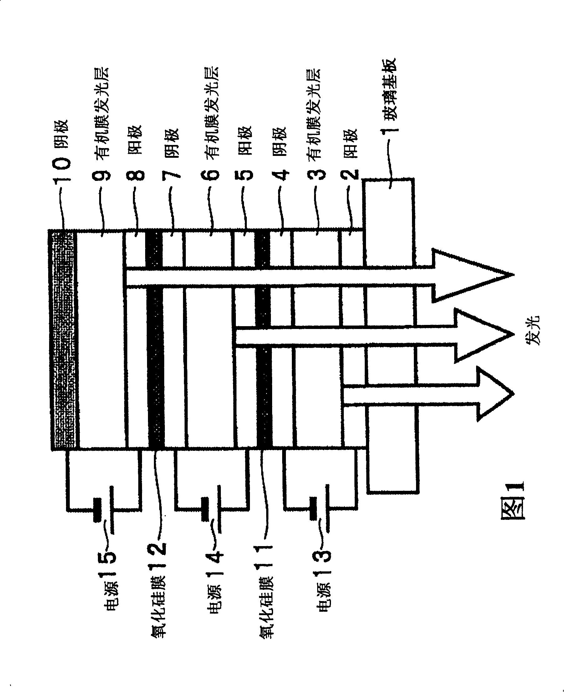
[0082] FIG. 1 shows a layer configuration of a pixel of a display device in a first embodiment of the present invention. The display device is, for example, an organic EL display. The glass substrate 1 is a display surface of a display device. The glass substrate 1 may be a plastic substrate as long as an organic film layer can be formed. An anode 2 is formed on the glass substrate 1 . As this anode 2, for example, ITO which is a transparent electrode, etc. can be used.
[0083] An organic film light emitting layer 3 is formed on the anode 2 . The organic film light emitting layer 3 is composed of a combination of a hole injection layer, a hole transport layer, an electron injection layer, an electron transport layer, and a light emitting layer composed of an organic compound as a phosphor. This combination must be properly selected according to the characteristics of organic EL.
[0084] A cathode 4 is formed on the organic film light emitting layer 3 . As the cathode 4...
no. 2 approach 》
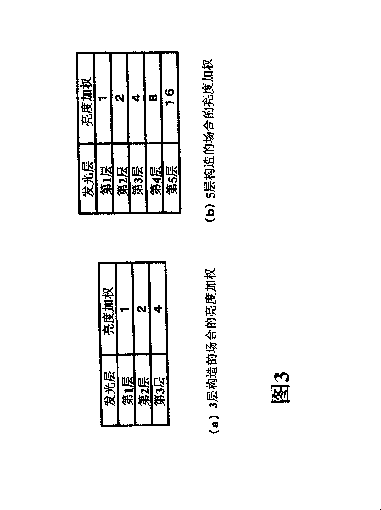
[0122] Next, the pixels in the display device according to the second embodiment of the present invention will be described in detail. In the above-mentioned first embodiment, each organic film light-emitting layer is formed of different materials that emit light with a predetermined luminance image, and the luminance is weighted. In the second embodiment, each organic film light-emitting layer is formed of the same material, and the value of current supplied to each organic film light-emitting layer and the time of supplying current are different to realize light emission with a predetermined brightness. Hereinafter, the specific configuration of the second embodiment and the luminance weighting methods of the first to seventh examples, which are suitable examples of the second embodiment, will be described in detail.
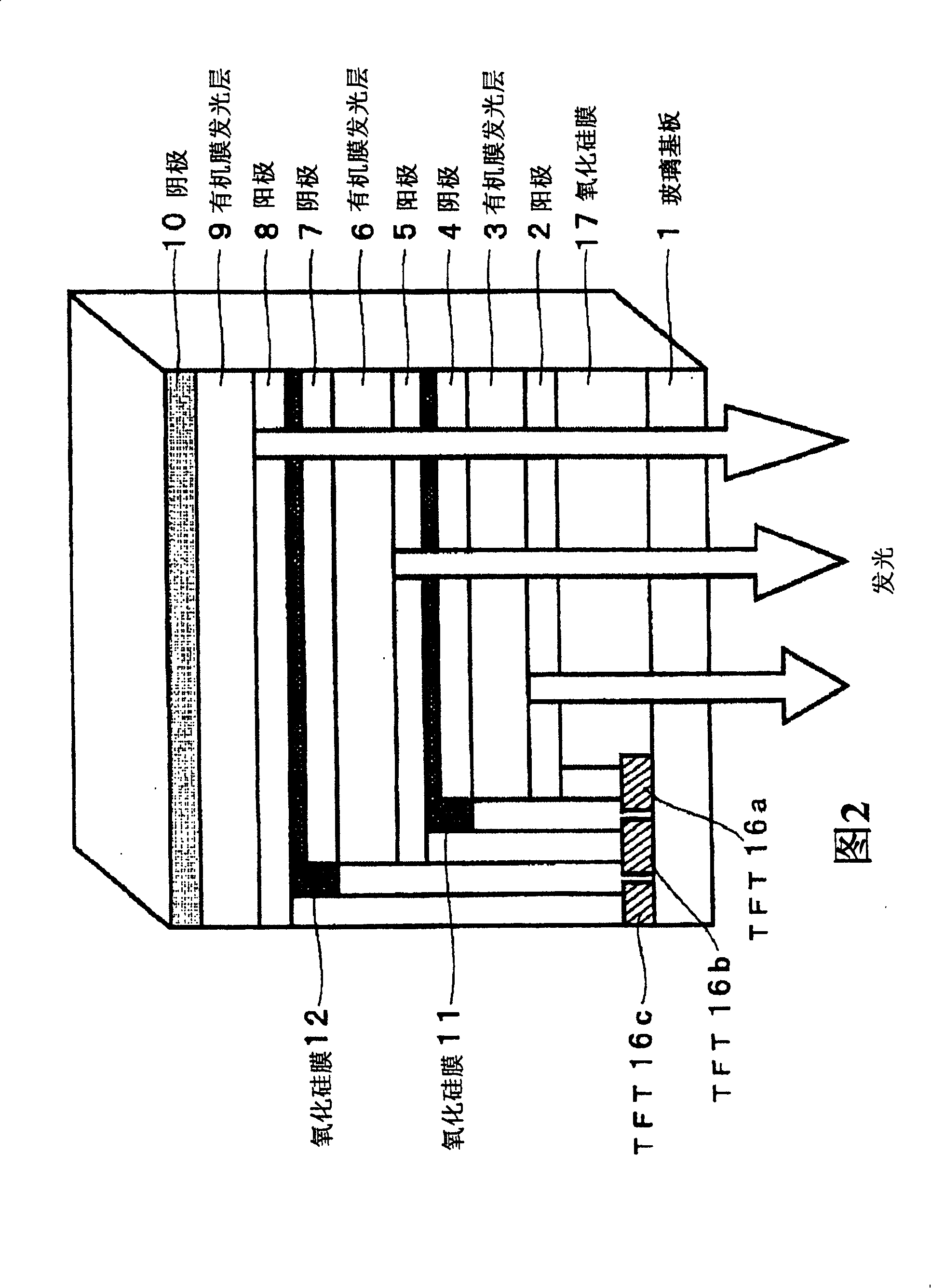
[0123] The layer configuration and pixel structure of the pixel are the same as those of the pixel of the first embodiment shown in FIGS. 1 and 2 , and thus d...
no. 1 example
[0132] First, an example in which different current values are flown to the organic EL light-emitting layers 18 , 19 , and 20 and weighted is shown. The turn-on time of TFTs 24-26 is T1=T2=T3=t.
[0133] Here, the current value of the current I1 flowing to the organic EL light emitting layer 18 is set to i, the current value of the current I2 flowing to the organic EL light emitting layer 19 is set to 2i, and the current value of the current I3 flowing to the organic EL light emitting layer 20 is set to 4i. . The current value thus set is supplied from the current control unit 900 and the power supply unit 381 ′ in the power supply circuit 38 .
[0134] In addition, the value of the current flowing to the organic EL light-emitting layers 18 to 20 is multiplied by the time length to become the luminance weight of each layer.
[0135] (weighted second embodiment)
[0136] Next, an example in which currents of the same current value flow to the organic EL light-emitting laye...
PUM
 Abstract
Description
Claims
Application Information
 - R&D
- Intellectual Property
- Life Sciences
- Materials
- Tech Scout
- Unparalleled Data Quality
- Higher Quality Content
- 60% Fewer Hallucinations
Browse by: Latest US Patents, China's latest patents, Technical Efficacy Thesaurus, Application Domain, Technology Topic, Popular Technical Reports.
© 2025 PatSnap. All rights reserved.Legal|Privacy policy|Modern Slavery Act Transparency Statement|Sitemap|About US| Contact US: help@patsnap.com