Flat display panel with thin film transistor

A thin-film transistor and flat-panel display technology, applied in transistors, electric solid-state devices, semiconductor devices, etc., can solve problems such as manufacturing process complexity

Active Publication Date: 2008-09-17
SAMSUNG DISPLAY CO LTD
View PDF12 Cites 0 Cited by
  • Summary
  • Abstract
  • Description
  • Claims
  • Application Information

AI Technical Summary

Problems solved by technology

However, according to the above method, the channel length has to be changed, thereby complicating the manufacturing process

Method used


Image

  • Flat display panel with thin film transistor
  • Flat display panel with thin film transistor
  • Flat display panel with thin film transistor

Examples


Embodiment Construction

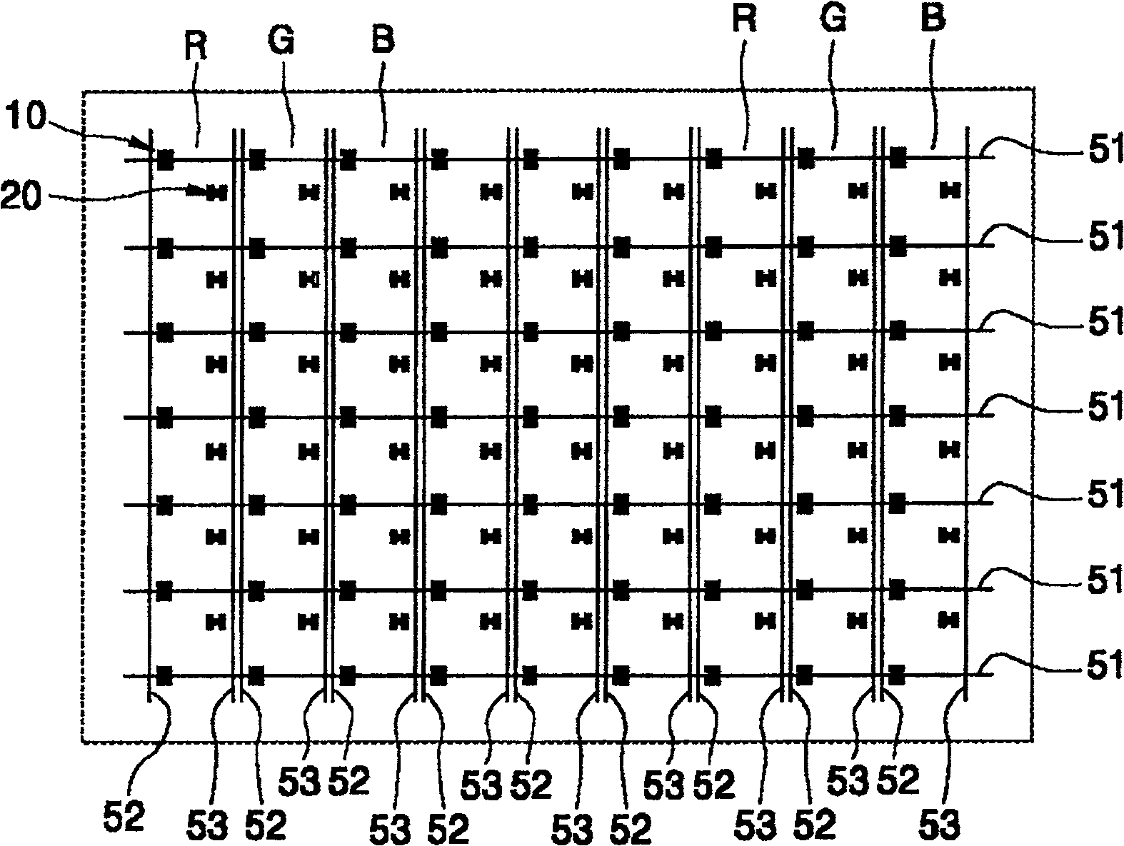
[0051] figure 1 is a plan view of an active layer structure of a thin film transistor (TFT) in an active matrix type organic electroluminescence display according to an embodiment of the present invention. exist figure 1 , the red (R), green (G), blue (B) sub-pixels are along the longitudinal direction ( figure 1 up and down direction) are repeatedly arranged in the pixels of the organic electroluminescent display. However, it should be understood that the arrangement of pixels is not limited to the above structure, and sub-pixels of each color may be arranged in various patterns such as a mosaic pattern or a grid pattern to form a pixel. Moreover, monochrome flat panel displays can be used instead of figure 1 Full color flat panel display shown.

[0052] In an organic electroluminescence display, a plurality of grid lines 51 are arranged along the lateral direction ( figure 1 The left-right direction in ) is arranged, and the plurality of data lines 52 are arranged in th...


PUM


Abstract

A flat panel display is provided. The flat panel display includes a light emitting device and two or more thin film transistors (TFTs) having semiconductor active layers having channel regions, where the thickness of the channel regions of the TFTs are different from each other. Thus, higher switching properties of a switching TFT can be maintained, a more uniform brightness of a driving TFT can be satisfied, and a white balance can be satisfied without changing a size of the TFT active layer.

Description

[0001] This application claims Korean Patent Application No. 2003-26004 filed with the Korean Intellectual Property Office on April 24, 2003, Korean Patent Application No. 2003-26007 filed with the Korean Intellectual Property Office on April 24, 2003, and Korean Patent Application No. Priority of Korean Patent Application No. 2003-27992 filed at the Korean Intellectual Property Office on June 1, and Korean Patent Application No. 2003-38826 filed at the Korean Intellectual Property Office on June 16, 2003, the entire contents of these disclosures It is listed here as a reference. technical field [0002] The present invention relates to active-matrix flat-panel displays comprising thin-film transistors (TFTs), and more particularly to flat-panel displays comprising TFTs having polysilicon as an active layer, and channels of the active layers in each TFT The regions have different thicknesses and different sized grains from each other. Background technique [0003] Thin film...

Claims


Application Information

Patent Timeline
Patent Type & Authority Patents(China)
IPC IPC(8): G09F9/30H01L29/78G02F1/1368H01L21/20H01L21/77H01L27/12H01L27/32H01L29/04H01L29/06H01L29/786H01L31/036
CPCH01L21/2026G02F1/1368H01L27/1285H01L29/04H01L27/3297H01L29/0684H01L27/1296H01L29/78696H01L27/1233H01L27/1229H01L21/02595H01L21/02686H01L21/02488H01L21/02422H01L21/02532H10K59/131H01L21/02675
Inventor 具在本朴志容朴惠香李基龙李乙浩
Owner SAMSUNG DISPLAY CO LTD
Why Eureka
Try Eureka