Thin film transistor array panel
A technology of thin film transistors and array panels, applied in nonlinear optics, instruments, optics, etc., can solve problems such as reducing the aperture ratio
- Summary
- Abstract
- Description
- Claims
- Application Information
AI Technical Summary
Problems solved by technology
Method used
Image
Examples
no. 2 example
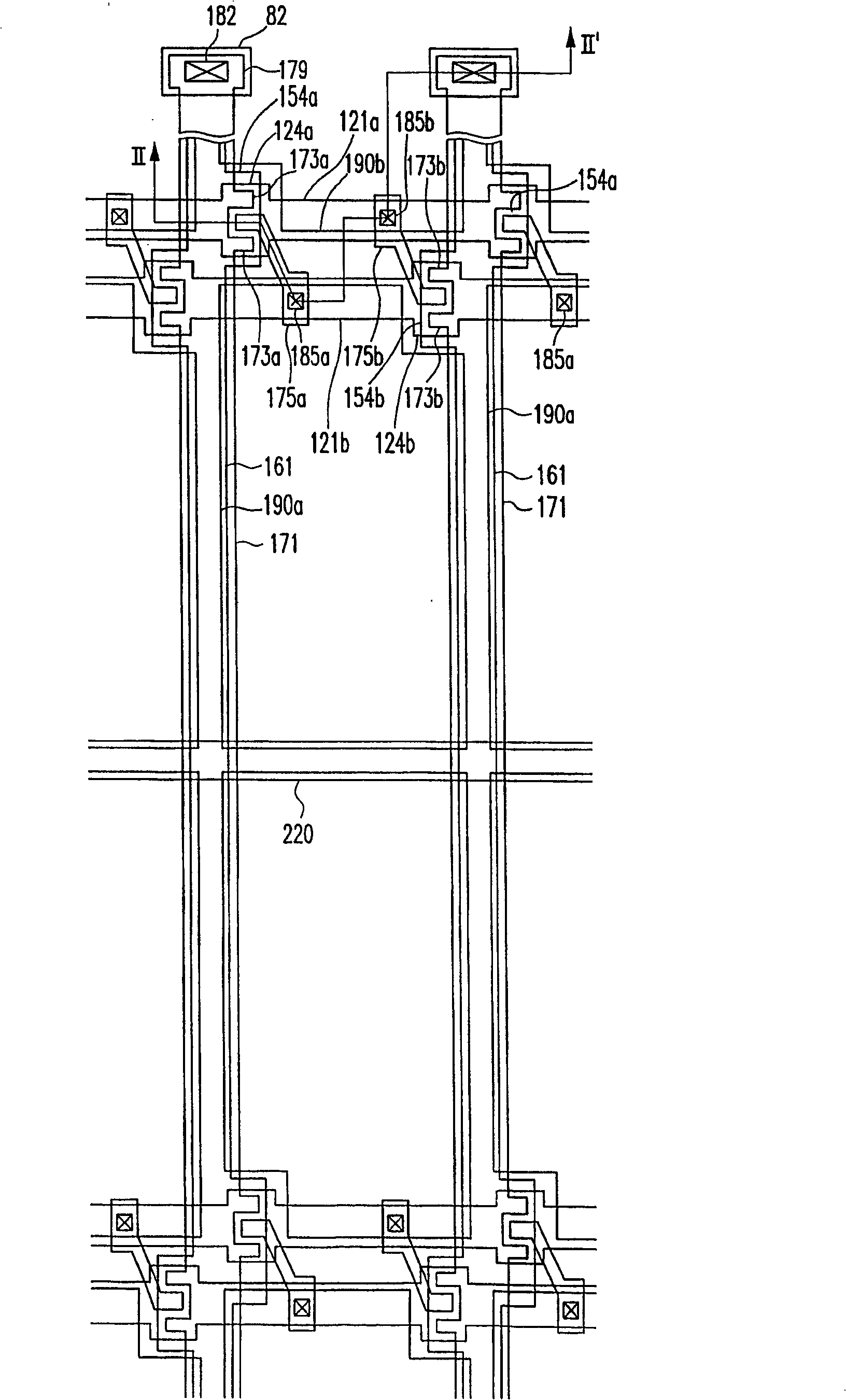
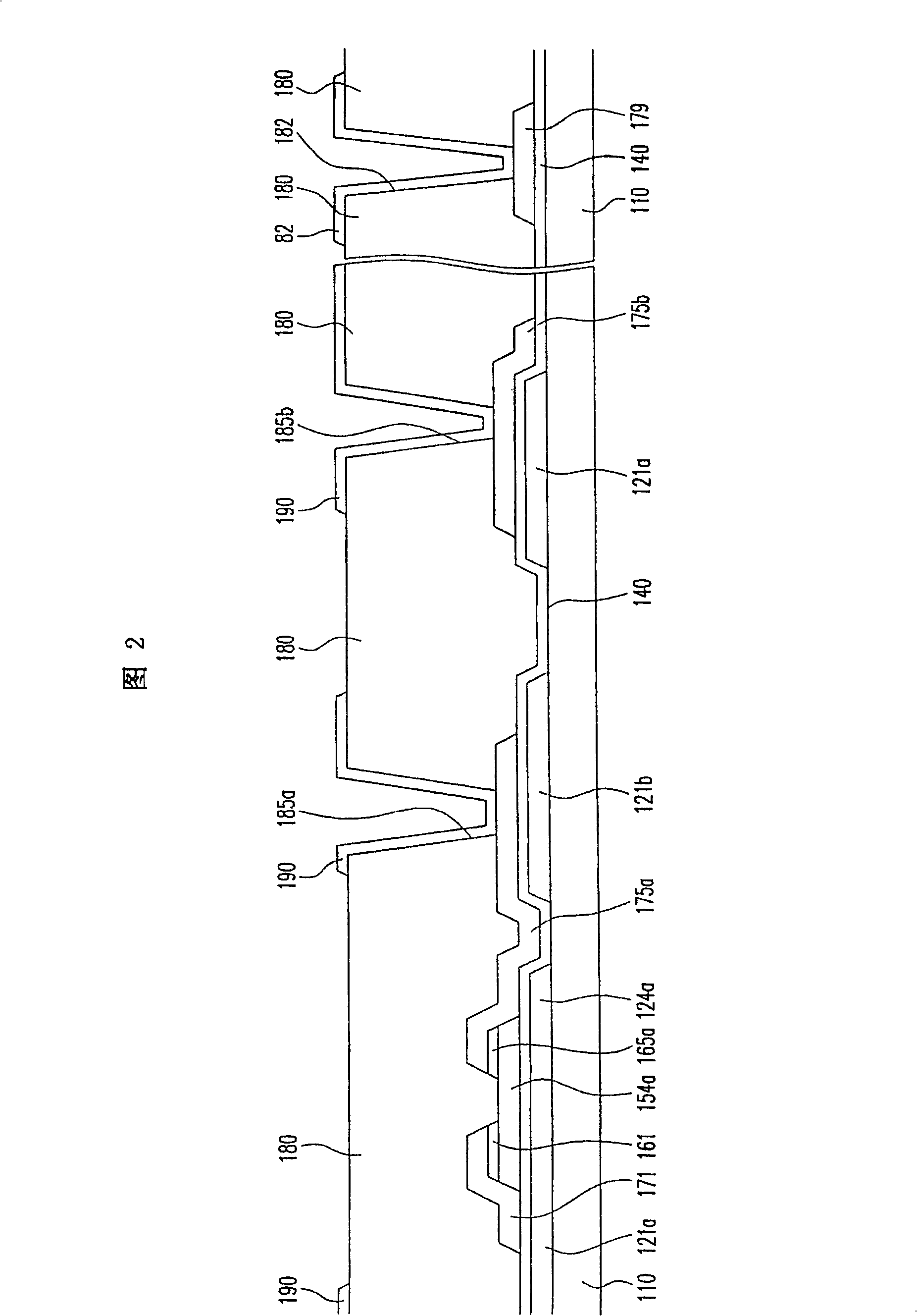
[0076] Unlike the above-described embodiments, the color filters are formed on the TFT array panel of the LCD. Such as Figure 11 As shown in FIG. 12, a TFT array panel according to another embodiment of the present invention has a layered structure, which is compatible with figure 1 Equivalent to the embodiment shown in FIG. 2 .
[0077] Figure 11 It is a layout diagram of a TFT array panel of an LCD according to another embodiment of the present invention, and FIG. 12 is taken along line XII-XII' Figure 11 The cross-sectional view of the TFT array panel shown in .
[0078] and figure 1Unlike the TFT array panel in FIG. 2, the color filters 230R, 230G, 230B are formed on the passivation layer 180p. The passivation layer 180p is made of an insulator such as silicon oxide or silicon nitride, and the passivation layer 180p protects the exposed portion of the semiconductor 154 and prevents a color agent from the color filter to another layer.
[0079] The color filters 23...
no. 3 example
[0092] Different thin films other than the color filter on the TFT array panel according to the above-described embodiments are formed of a photoresist film, and the formation of the different thin films will be described in detail with reference to the accompanying drawings.
[0093] Figure 17 It is a layout diagram of a TFT array panel of an LCD according to another embodiment of the present invention, and FIG. 18 is taken along the line XII-XII' Figure 17 The cross-sectional view of the TFT array panel shown in . Figure 19 is an intermediate step in the manufacturing method of the TFT array panel according to the embodiment of the present invention Figure 17 and a sectional view of the TFT array panel shown in FIG. 18 , and FIG. 20 is a sectional view in the next step of the steps shown in FIG. 19 , Figure 21 is the layout diagram in the next step of the steps shown in Fig. 20, and Fig. 22 is taken along the line XVb-XVb' Figure 21 A cross-sectional view of the TFT ...
PUM
 Abstract
Description
Claims
Application Information


