

Semiconductor device
a technology of semiconductors and devices, applied in the direction of non-linear optics, radio-controlled devices, instruments, etc., can solve the problems of large off current (current flowing when the tft is in an off state), character degradation, and inability to adapt to circuits
- Summary
- Abstract
- Description
- Claims
- Application Information
AI Technical Summary
Benefits of technology
Problems solved by technology
Method used
Image

Examples
embodiment mode 1
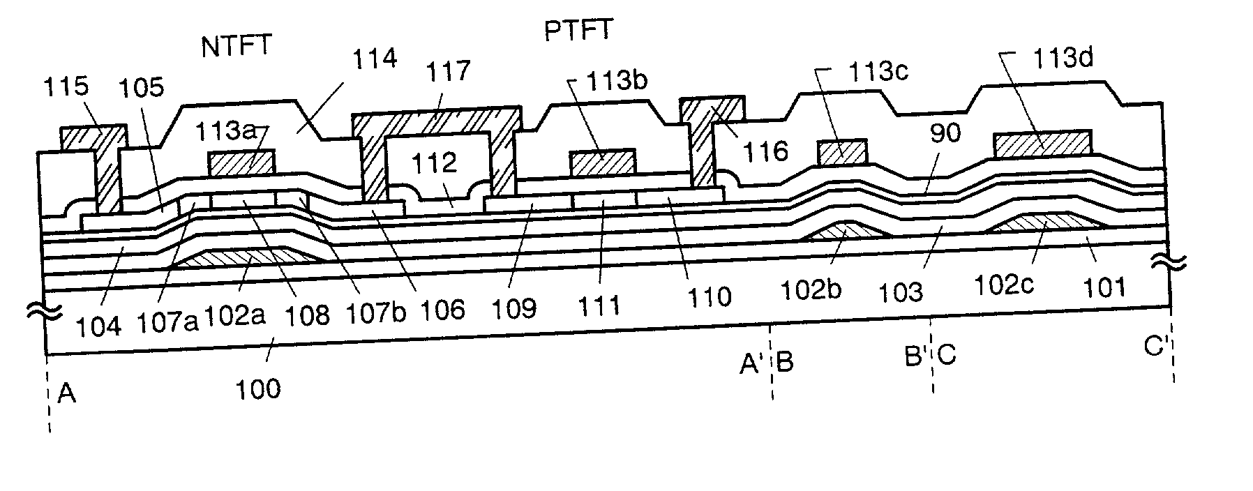
[0039] An embodiment mode of the present invention will be described taking as an example a CMOS circuit (inverter circuit) in which an n-channel TFT (hereinafter referred to as NTFT) is combined with a p-channel TFT (hereinafter referred to as PTFT).
[0040] A sectional structure thereof is shown in FIG. 1A and a top view thereof is shown in FIG. 1B. The description will be given using symbols common to FIGS. 1A and FIG. 1B. The sectional views taken along the lines A-A', B-B', and C-C' in FIG. 1B correspond to the sectional views A-A', B-B', and C-C' in FIG. 1A, respectively.
[0041] In FIG. 1A, 100 denotes a substrate; 101, a base film; 102a, 102b, and 102c, first wiring lines; 103, a first insulating layer; 104, a second insulating layer; and 90, a silicon oxide film to serve as a base of active layers. An active layer of the NTFT is composed of a source region 105, a drain region 106, low concentration impurity regions (LDD regions) 107a and 107b, and a channel formation region 108...
embodiment mode 2
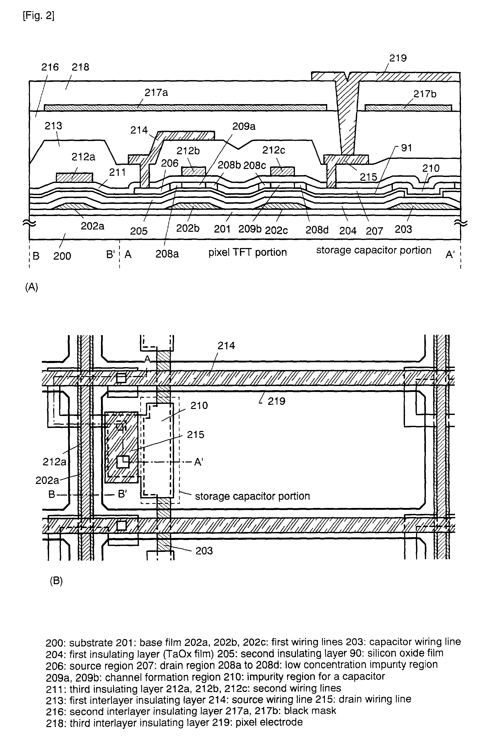
[0055] An embodiment mode of the present invention will be described taking as an example a pixel matrix circuit that uses an NTFT for a pixel TFT. This pixel matrix circuit is formed on the same substrate as the CMOS circuit described in Embodiment Mode 1 at the same time. Therefore, see the description in Embodiment Mode 1 for details of the wiring lines denoted by the identical names.
[0056] A sectional structure of the pixel matrix circuit is shown in FIG. 2A and a top view thereof is shown in FIG. 2B. The description will be given using symbols common to FIG. 2A and FIG. 2B. The sectional views taken along the lines A-A' and B-B' in FIG. 2B correspond to the sectional views A-A' and B-B' in FIG. 2A, respectively.
[0057] In FIG. 2A, 200 denotes a substrate, 201, a base film, 202a to 202c, first wiring lines, 203, a capacitor wiring line, 204, a first insulating layer, 205, a second insulating layer, and 91, a silicon oxide film to serve as a base of an active layer. An active laye...
embodiment 1
[0075] [Embodiment 1]
[0076] In this embodiment, a method of manufacturing the CMOS circuit described in Embodiment Mode 1 will be described. The description will be given with reference to FIG. 3.
[0077] First, a glass substrate is prepared as a substrate 300. A silicon oxide film with a thickness of 200 nm is formed thereon by sputtering as a base film 301. On the base film, first wiring lines 302a, 302b, and 302c are formed. The material of the first wiring lines is a tantalum film formed by sputtering. An oxide film may be formed on a surface of the tantalum film.
[0078] Other metal films, alloy films, or a laminate of those may of course be used because the first wiring lines 302a, 302b, and 302c can be formed of any film as long as it has conductivity. A film that can be formed by patterning with a small taper angle is effective in improving the levelness.
[0079] Next, a tantalum oxide film is formed again by sputtering. In this embodiment, the thickness thereof is set to 10 to 50...
PUM
 Abstract
Description
Claims
Application Information