
Semiconductor device

a semiconductor and display device technology, applied in the direction of identification means, instruments, non-linear optics, etc., can solve the problems of defective display, deterioration of image quality and contrast, and generating optical leakage current by optical excitation

Inactive Publication Date: 2008-12-16
SEMICON ENERGY LAB CO LTD
View PDF46 Cites 8 Cited by
  • Summary
  • Abstract
  • Description
  • Claims
  • Application Information

AI Technical Summary

Benefits of technology

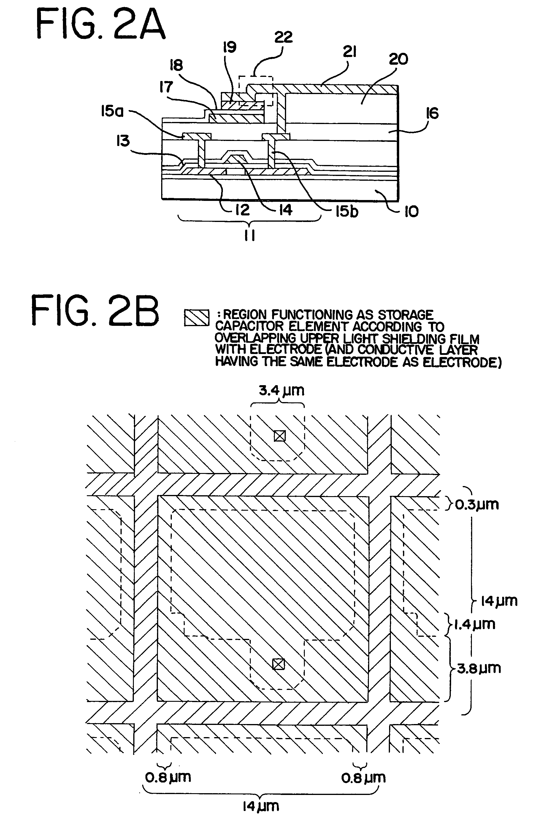
The present invention provides a semiconductor device with a capacitor element that can obtain a sufficient storage capacitor without reducing an opening ratio. The device includes a thin film transistor, a storage capacitor element, a light-shielding film, a capacitor insulating film, a conductive layer, an insulating film, and a pixel electrode. The conductive layer and the pixel electrode are brought into contact with each other through an opening formed in the insulating film. The light-shielding film is formed on the thin film transistor and the conductive layer is formed on the light-shielding film. The insulating film is formed so that a step of the pixel electrode caused by the conductive layer and the capacitor insulating film is flattened. The conductive layer is electrically connected to the pixel electrode and the storage capacitor element is composed of the light-shielding film, the capacitor insulating film, and the conductive layer. The flattening film is formed to prevent defects in orientation of liquid crystal caused by steps or unevennesses on the surface of the pixel electrode. The invention provides a semiconductor device with a sufficient storage capacitor without reducing an opening ratio.

Problems solved by technology

Thus, it is important to hold a charge (signal) and even a slight amount of leak current generated during a holding time at which the TFT is in an OFF state causes a deterioration of an image quality and a decrease in a contrast.
However, the TFT involves such a problem that when a semiconductor layer is irradiated with a light, optical excitation occurs to generate an optical leakage current.
However, in the liquid crystal display device, there arises a problem in that a defective display is caused by a defect in orientation of the liquid crystal.
Steps or unevennesses on the surface of the pixel electrode affect the surface of an orientation film and involve uneven rubbing on the orientation film, and finally causes the defect in orientation of the liquid crystal and the deterioration of the image quality.
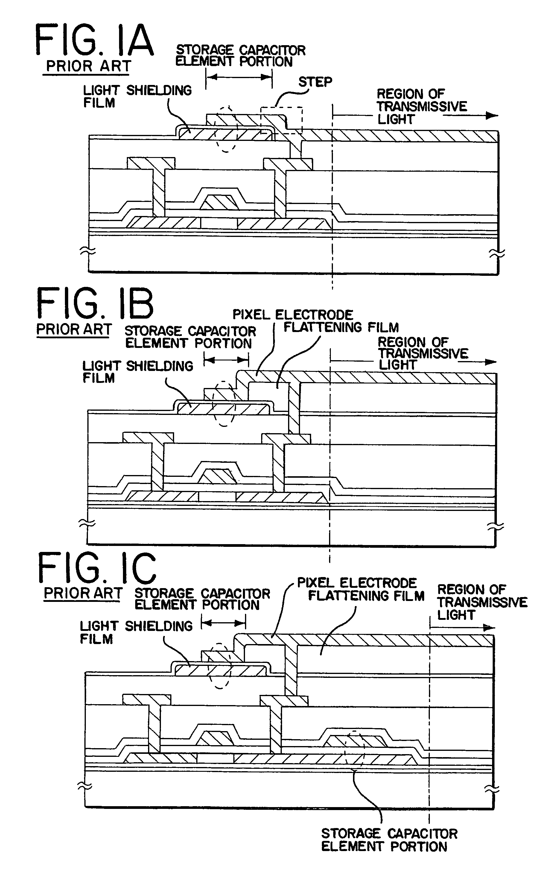
In the structure disclosed in JP 2924506 B, as shown in FIG. 1A, the step of the pixel electrode exists in a portion outside a light-shielded region by the light-shielding film (a region transmissive of light) and there arises a problem in that the light accidentally passes therethrough due to the defect in orientation of the liquid crystal, or the like.
However, in the display device including a laminate structure consisting of a number of layers, it is unavoidable that the steps or unevennesses occur on the surface of the pixel electrode and affect the surface of the orientation film as well, followed by decrease in the contrast due to a light accidentally passing therethrough.
However, according to this method, when the storage capacitor element is formed between the light-shielding film and the pixel electrode, as shown in FIG. 1B, an interlayer distance is made large between the light-shielding film and the pixel electrode to thereby make a region functioning as the capacitor element narrow, with the result that it is impossible to secure the sufficient storage capacitor.
Due to a slight amount of off-leak current flowing while the TFT is in an OFF state, the decrease in the contrast and a nonuniform image quality as a panel are caused, so that it is unavoidable that the storage capacitor element is formed for complementation thereof.

Method used


Image

  • Semiconductor device
  • Semiconductor device
  • Semiconductor device

Examples


embodiment 1

[0054]A method of manufacturing an active matrix substrate is explained in Embodiment 1 using FIGS. 4A to 6. A substrate on which driver circuits, and a switching element in the pixel portion (the pixel TFTs) and storage capacitor elements are formed is referred to as an active matrix substrate in Embodiment 1, for convenience.

[0055]First, a substrate made from glass, such as barium borosilicate glass or aluminum borosilicate glass, typically Corning Corp. #7059 glass, #1737 glass, and the like is used as a substrate in Embodiment 1. Note that quartz substrates, silicon substrates, and metallic substrates and stainless steel substrates on which an insulating film is formed may also be used as the substrate. Further, plastic substrates having heat resistant properties capable of withstanding the processing temperatures of Embodiment 1 may also be used. A quartz glass substrate is applied in Embodiment 1.

[0056]A lower portion light shielding film 101 is formed next on the quartz subst...

embodiment 2

[0087]In Embodiment 2, the manufacturing method of the semiconductor device of different structure from Embodiment 1 is described with reference to FIG. 7.

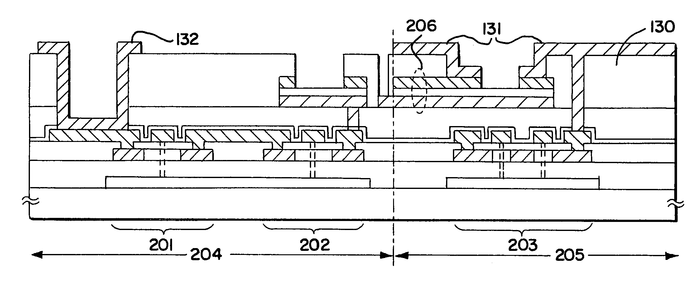
[0088]The pixel electrode 131 electrically connected with the conductive layer 128 is formed on the planarizing film 130 according to Embodiment 1. Then, the large level difference formed between the adjoining pixels which are generated by the light shielding film 124 formed on the second interlayer insulating film 123, the capacitor insulating film 126, the conductive layer 128, and pixel electrode 131 is planarized with the insulating film 401 which consists of acrylics, polyimide and the like as shown in FIG. 7. Subsequently, although the alignment film 402 is formed, since the level difference between the adjoining pixels is buried and planarized by the insulating film 401, it is hard to produce unevenness on the alignment film 402 surface. Then, rubbing processing is performed and the substrate and opposite substrate in which...

embodiment 3

[0090]In Embodiment 3, the manufacturing method of semiconductor device of different structure from Embodiment 1 with reference to FIG. 8.

[0091]The light shielding film 301, the capacitor insulating film 302, and the conductive layer 303 according to Embodiment 1. Then, shown by the arrow of FIG. 8A, the electric conduction layer 303 is etched so that it becomes inside a little from the light shielding film 301 and the capacitor insulating film 302. The etching is performed by using masks, or over etching may be performed. It can prevent the generation of leak current due to the conductive layer 303 being contact with the light shielding film 301.

[0092]Furthermore, by carrying out over etching the light shielding film 311, the capacitor insulating film 312, and the conductive layer 313 in this order so as to be in a staircase order as shown in FIG. 8B. By carrying out etching using a mask, laminating can be made gently-sloping and the level difference and unevenness of pixel electro...


PUM

PropertyMeasurementUnit
sizeaaaaaaaaaa
areaaaaaaaaaaa
areaaaaaaaaaaa

Abstract

To realize a semiconductor device including a capacitor element capable of obtaining a sufficient capacitor without reducing an opening ratio, in which a pixel electrode is flattened in order to control a defect in orientation of liquid crystal. A semiconductor device of the present invention includes a light-shielding film formed on the thin film transistor, a capacitor insulating film formed on the light-shielding film, a conductive layer formed on the capacitor insulating film, and a pixel electrode that is formed so as to be electrically connected to the conductive layer, in which a storage capacitor element comprises the light-shielding film, the capacitor insulating film, and the conductive layer, whereby an area of a region serving as the capacitor element can be increased.

Description

[0001]This application is a continuation of U.S. application Ser. No. 10 / 254,280, filed on Sep. 25, 2003 now U.S. Pat. No. 6,831,297.BACKGROUND OF THE INVENTION[0002]1. Field of the Invention[0003]The present invention relates to a liquid crystal display device in which a semiconductor device such as a transistor formed on an insulator, in particular, a field effect transistor, and typically a MOS (metal oxide semiconductor) transistor, a thin film transistor (hereinafter, referred to as TFT) is used as a switching element in a pixel portion. The present invention also relates to a liquid crystal display device including a circuit or a driving circuit manufactured by using the semiconductor device, and to an electric appliance in which the liquid crystal display device is used for a display portion.[0004]2. Description of the Related Art[0005]Recently, there has been growing a use of the liquid crystal display device in a monitor of a personal computer or a display device of a telev...

Claims


Application Information

Patent Timeline
Patent Type & Authority Patents(United States)
IPC IPC(8): H01L29/04G02F1/1368G02F1/1333G02F1/1335G02F1/1343G02F1/1362G09F9/00G09F9/30H01L21/336H01L21/77H01L21/84H01L27/12H01L27/13H01L29/786
CPCG02F1/136209H01L27/124H01L29/66765H01L29/78633H01L27/1255H01L29/66757G02F1/136213G02F1/136227
Inventor ARAO, TATSUYA
Owner SEMICON ENERGY LAB CO LTD
Learn More