Dynamic random access memory and mfg. method thereof

A dynamic random access and memory technology, which is applied in semiconductor/solid-state device manufacturing, transistors, electrical components, etc., can solve the problems affecting the reliability of components, the starting voltage deviation of active components, and the increase of field junction leakage current, etc., to achieve Improve the integration of components, simplify the process, and increase the effect of process margin

Active Publication Date: 2008-12-24
PROMOS TECH INC
View PDF2 Cites 0 Cited by
  • Summary
  • Abstract
  • Description
  • Claims
  • Application Information

AI Technical Summary

Problems solved by technology

[0007] However, in the above-mentioned DRAM, since the active element 106 is usually produced by a lithographic etching process, the length d of the channel region of the active element 106 will be limited by the lithographic etching process and cannot be further refined. Shrinking, so that the component integration level cannot be further improved
On the other hand, the reduction of the length d of the channel region will also cause the problem of the starting voltage deviation of the active element and the so-called short channel effect.
In order to solve the above problems, an existing method is to increase the dopant concentration in the channel of the active device, but this method will increase the field junction leakage current (field junction leakage) and affect the reliability of the device.

Method used


Image

  • Dynamic random access memory and mfg. method thereof
  • Dynamic random access memory and mfg. method thereof
  • Dynamic random access memory and mfg. method thereof

Examples


Embodiment Construction

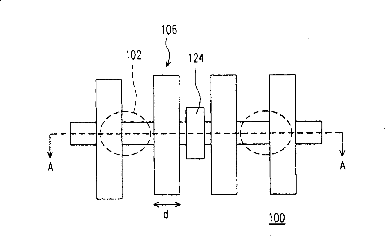
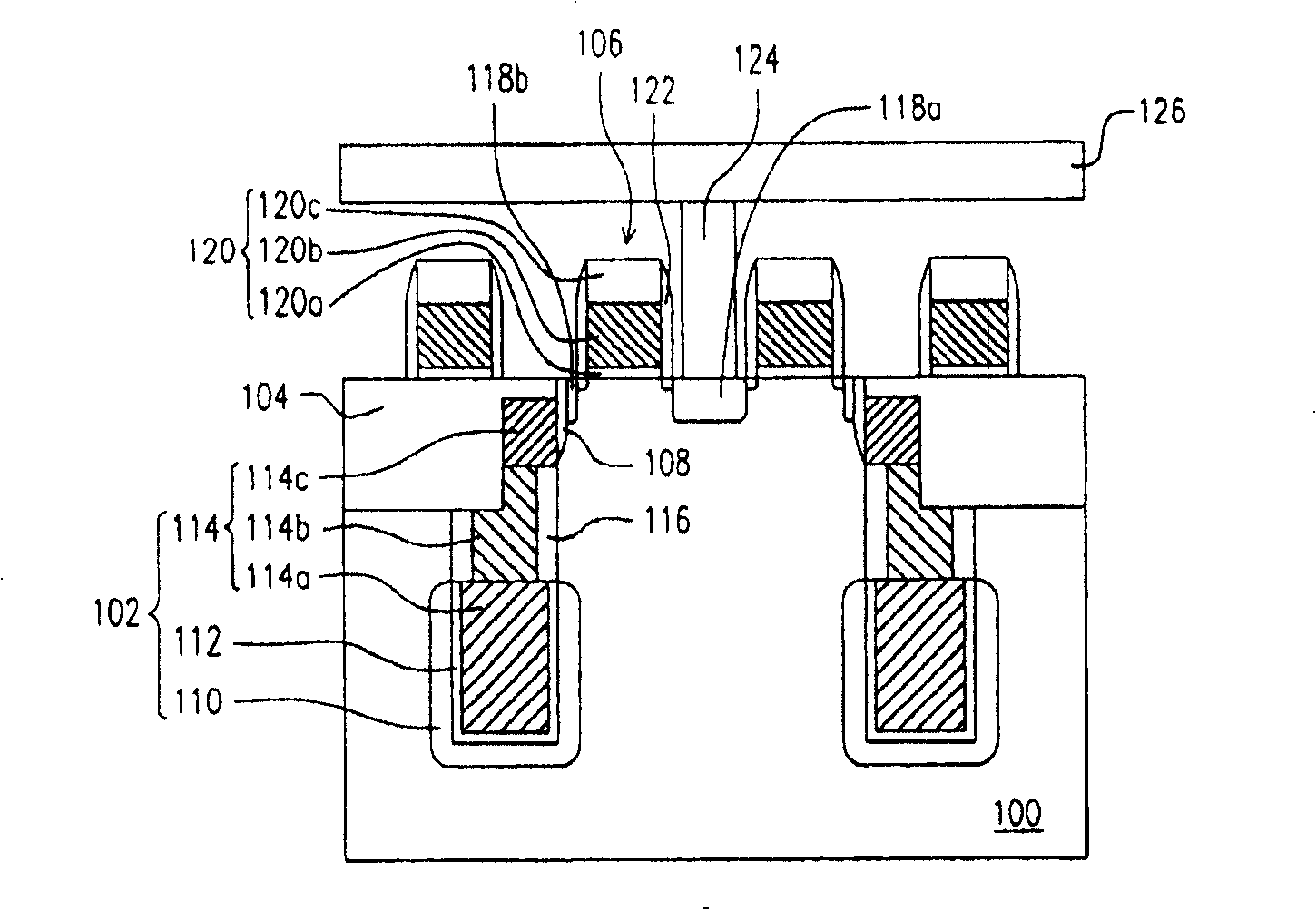
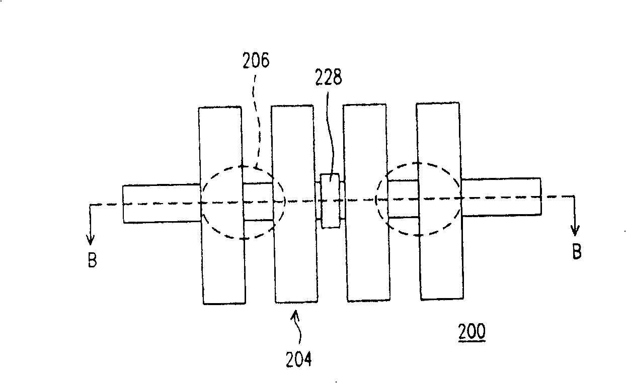
[0078] Figure 2A Shown is a top view of a deep trench DRAM according to a preferred embodiment of the present invention. Figure 2B Shown is a cross-sectional view of the deep trench dynamic random access memory of the present invention, wherein Figure 2B depicted as Figure 2A The section along the line B-B'.

[0079] Please refer to Figure 2A and Figure 2B , the dynamic random access memory includes a substrate 200 , an element isolation structure 202 , an active element 204 and a deep trench capacitor 206 .

[0080] The substrate 200 is, for example, a silicon substrate. For example, deep trenches 208 and shallow trenches 210 are disposed in the substrate 200 . The depth of the deep trench 208 is, for example, greater than the depth of the shallow trench 210 .

[0081] The device isolation structure 202 is, for example, disposed on the substrate 200 to define an active region. The device isolation structure 202 is, for example, a shallow trench isolation structu...


PUM


Abstract

The invention is a dynamic random access memory (DRAM), comprising substrate, active component and deep tunnel capacitor, where the substrate has tunnel and deep tunnel; the active component is arranged on the substrate and comprises grid structure and doping region, the grid structure is arranged on the substrate and filled in the tunnels and the doping region is arranged in the substrate on the first side of the grid; the deep tunnel capacitor is arranged in the deep tunnel in the substrate on the second side of the grid; the first and second sides are opposite to each other; and electrodes on the deep tunnel capacitor are adjacent to the tunnel bottom.

Description

technical field [0001] The present invention relates to a semiconductor element and its manufacturing method, and in particular to a dynamic random access memory and its manufacturing method. Background technique [0002] As the functions of today's computer microprocessors (Microprocessor) become more and more powerful, the programs and calculations performed by software are also becoming more and more complex. Therefore, memory manufacturing technology has become one of the important technologies in the semiconductor industry. [0003] In general, memory can be classified into volatile memory and non-volatile memory according to the type of data stored therein. A dynamic random access memory (Dynamic Random Access Memory, DRAM) is a kind of volatile memory, and it is composed of a plurality of storage units. Each memory cell is composed of an active element and a capacitor, and each memory cell is electrically connected to each other through a word line (WL, WL) and a bi...

Claims


Application Information

Patent Timeline
Patent Type & Authority Patents(China)
IPC IPC(8): H01L27/108H01L21/8242
Inventor 简荣吾
Owner PROMOS TECH INC
Why Eureka
Try Eureka