
III group nitride semiconductor LED based on plane structure and its preparing process

A technology for nitride semiconductors and light-emitting diodes, applied in semiconductor devices, electrical components, circuits, etc., can solve the problems of high manufacturing cost, difficulty in making diodes with large light-emitting area, and increased process cost.

Inactive Publication Date: 2009-06-17
NANJING UNIV
View PDF3 Cites 0 Cited by
  • Summary
  • Abstract
  • Description
  • Claims
  • Application Information

AI Technical Summary

Problems solved by technology

Their manufacture usually requires selective etching of the nitride luminescent material to expose the electrical contact area, which requires multi-step photolithography, plasma etching and other steps, and thus has a relatively high manufacturing cost; and due to the need for p-type The ohmic contact is made separately on the n-type nitride material, and the process cost is further increased.
At the same time, it is difficult to make a diode with a large light-emitting area due to the limitation of the electrode size
Finally, due to the asymmetric structure of the device, the above light-emitting diodes can only be driven by DC, so an additional AC-DC conversion circuit must be added between the AC source and the device, which increases the cost of device application
At present, the high cost is the main reason why III-nitride semiconductor light-emitting diodes are still difficult to enter the conventional lighting market on a large scale

Method used


Image

  • III group nitride semiconductor LED based on plane structure and its preparing process
  • III group nitride semiconductor LED based on plane structure and its preparing process
  • III group nitride semiconductor LED based on plane structure and its preparing process

Examples


Embodiment Construction

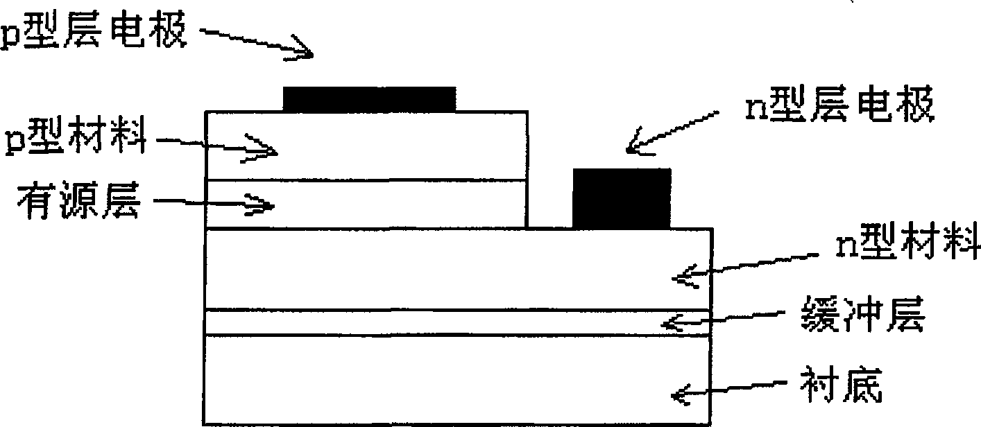
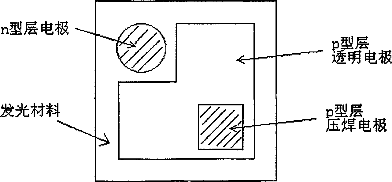
[0028] To further illustrate the content of the present invention, the present invention will be described in detail below in conjunction with the embodiments and accompanying drawings. Among them: see figure 1 and figure 2 As shown, the fabrication process of the usual vertical structure Group III nitride semiconductor light-emitting diode is:

[0029] 1) growing buffer layers, active light-emitting layers and contact layers based on group III nitride semiconductor materials on sapphire or silicon substrates by chemical vapor deposition;

[0030] 2) Expose the electrical contact area on the other side of the active area of ​​the light-emitting diode by etching. figure 1 , figure 2 The middle finger engraves the electrical contact area of ​​n-type material;

[0031] 3) Fabricate n-type layer and p-type layer electrodes in the electrical contact region for n-type and p-type materials respectively by using semiconductor process technology.

[0032] see image 3 and Fig...


PUM

PropertyMeasurementUnit
thicknessaaaaaaaaaa
thicknessaaaaaaaaaa
thicknessaaaaaaaaaa

Abstract

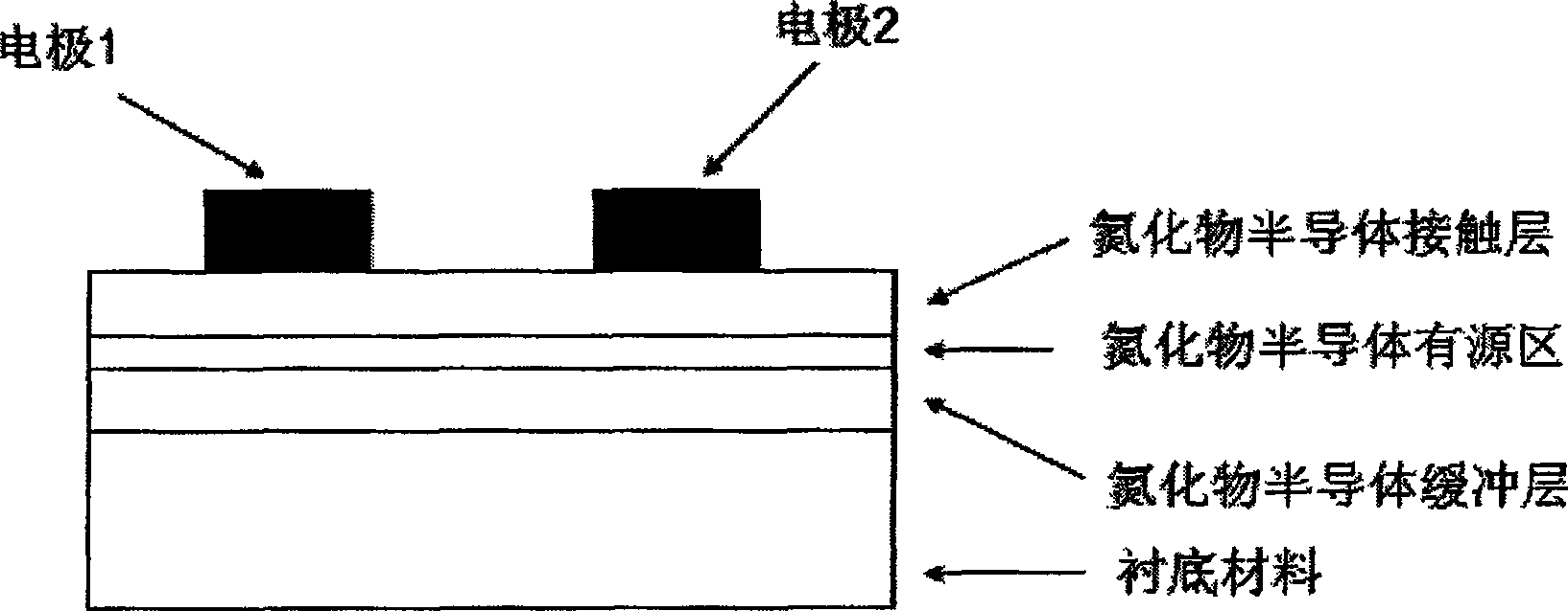
A III-nitride semiconductor luminescence diode based on a plane structure is provided with a nitride semiconductor buffer layer, a nitride semiconductor active layer and a nitride semiconductor contact layer on the substrate materials respectively, and two legato electrodes are arranged on the contact layer which is at the same side with the nitride semiconductor active layer; the buffer layer is the monolayer or multilayer structure with various components, the material of the buffer layer is nitride aluminum gallium and indium and the whole thickness thereof is between 0.01-100 Mum; and the buffer layer can adopt the unintentional doping, N-type doping or P-type doping during the growing period; the material of the active layer, the thickness of which is 0.001-10 Mum, is nitride aluminum gallium indium with the monolayer or multilayer structure of various components; the material of contact layer, the thickness of which is between 0.001-10 Mum, is nitride aluminum gallium indium with the monolayer or multilayer structure of various components, and the electrode is the schottky contact or ohmic contact electrode.

Description

1. Technical field [0001] The invention relates to a semiconductor light-emitting diode and a preparation method thereof, in particular to a group III nitride semiconductor light-emitting diode based on a planar structure and a preparation method thereof. 2. Background technology [0002] Group III nitride semiconductors (including AlN, GaN, InN and their alloys) are direct bandgap semiconductors, and the bandgap covers from infrared to ultraviolet regions, with high electron mobility, excellent thermal stability and chemical stability. Stability, can withstand a strong electric field, and can form a variety of heterogeneous structures, which can be used to manufacture visible light-emitting diodes of various colors, as well as ultraviolet light-emitting diodes. Solid-state light-emitting diodes made of such materials have the advantages of small size, light weight, high luminous efficiency, good device reliability, low power consumption, and easy modulation and integration....

Claims


Application Information

Patent Timeline
Patent Type & Authority Patents(China)
IPC IPC(8): H01L33/00H01L33/36
Inventor 陆海苗操张荣郑有炓
Owner NANJING UNIV
Learn More