Phase change film material of silicon-adulterated sulfur series for phase change memory
A technology of phase-change memory and chalcogenide, which is applied in the field of materials in the field of microelectronics technology, can solve the problems of affecting the contact between phase-change thin films and electrodes or other film layers, affecting the stability of devices, and unfavorable device operation, so as to reduce write The effect of operating current, improving life, and good energy transmission
- Summary
- Abstract
- Description
- Claims
- Application Information
AI Technical Summary
Problems solved by technology
Method used
Image
Examples
Embodiment 1
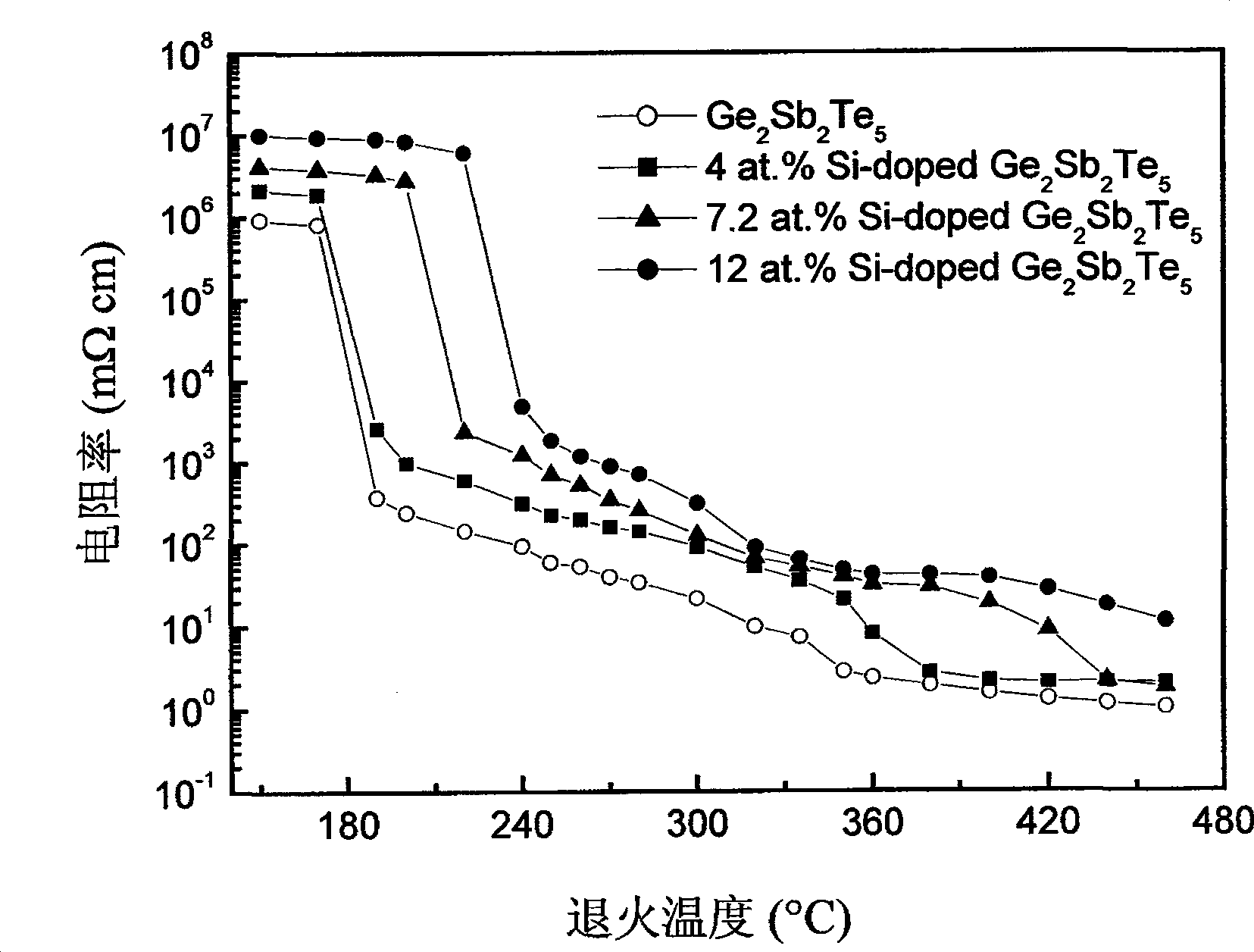
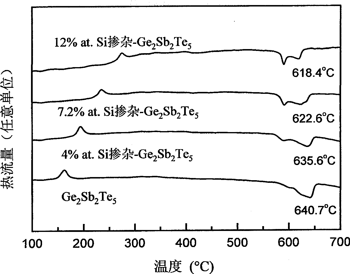
[0026] The phase change material series is Si doped into Te a Ge b Sb 100-(a+b) Alloy Si-doped Ge-Sb-Te films. The ranges of parameters a and b are proposed with reference to the parameter ranges of the patents of S.R.Ovshinsky et al. on phase change memory. figure 2 Si doped Ge obtained for different Si doping amounts 2 Sb 2 Te 5 Thin films and commonly used Ge 2 Sb 2 Te 5 The relationship between film resistivity and annealing temperature. At a temperature of 160°C and below, all films are in an amorphous state, and the film resistance is in a high resistance state. As the annealing temperature increases, the film begins to crystallize, and the film resistivity begins to decrease. When the film is crystallized, the film resistance is in a low resistance state. This process is realized in the device by heating the phase-change film with electric pulses, and the reversible transition between the high-resistance state and the low-resistance state can be achieved by a...
Embodiment 2
[0033] The phase change material series is a Si-Sb-Te alloy film formed by completely replacing the Ge element in the Ge-Sb-Te alloy with Si element. Figure 4 For the Si-Sb-Te chalcogenide film of the present invention and the commonly used Ge 2 Sb 2 Te 5 The relationship between film resistivity and annealing temperature. At a temperature of 160°C and below, all films are in an amorphous state, and the film resistance is in a high resistance state. As the annealing temperature increases, the film begins to crystallize, and the film resistivity begins to decrease. When the film is crystallized, the film resistance is in a low resistance state. This process is realized in the device by heating the phase-change film with electric pulses, and the reversible transition between the high-resistance state and the low-resistance state can be achieved by applying different electric pulses. Si-Sb-Te alloy thin films compared with commonly used Ge 2 Sb 2 Te 5 thin film, its amorp...
Embodiment 3
[0042] Both Ge element and Si element are group IV elements and have the same valence in the alloy, so the element Si can partially or even completely replace the Ge element in the Ge-Sb-Te alloy. When the Si element completely replaces the Ge element, it forms an implementation Si-Sb-Te alloy thin films described in Example 2. Si elements partially replace Te a Ge b Sb 100-(a+b) The Ge element in the alloy can form Te a Ge b-c Si c Sb 100-(a+b) alloy film. With reference to the experimental results of Example 1 and Example 2, it can be seen that the partial replacement of Ge elements by Si elements can still achieve the following effects: (1) improve the amorphous / crystalline resistance change rate of the film, thereby improving the on / off of the device Compare. (2) At the same time, the crystalline resistance of the thin film is appropriately increased, so as to achieve the purpose of reducing the writing operation current. (3) Lower the melting point of the film. ...
PUM
 Abstract
Description
Claims
Application Information


