Plane luminous element and method for manufacturing same

A technology for light-emitting components and manufacturing methods, which is applied in the manufacturing of semiconductor/solid-state devices, electrical components, electroluminescent light sources, etc. Longevity, the effect of improving quantum efficiency

Inactive Publication Date: 2009-09-16
RITDISPLAY
View PDF11 Cites 0 Cited by
  • Summary
  • Abstract
  • Description
  • Claims
  • Application Information

AI Technical Summary

Problems solved by technology

[0014] Another object of the present invention is to provide a planar light-emitting element and its manufacturing method, so as to solve the problems of inability to mass-produce, greatly increase the cost and limit the miniaturization of the element in the known methods of improving the external quantum efficiency of the element

Method used


Image

  • Plane luminous element and method for manufacturing same
  • Plane luminous element and method for manufacturing same
  • Plane luminous element and method for manufacturing same

Examples


no. 1 example

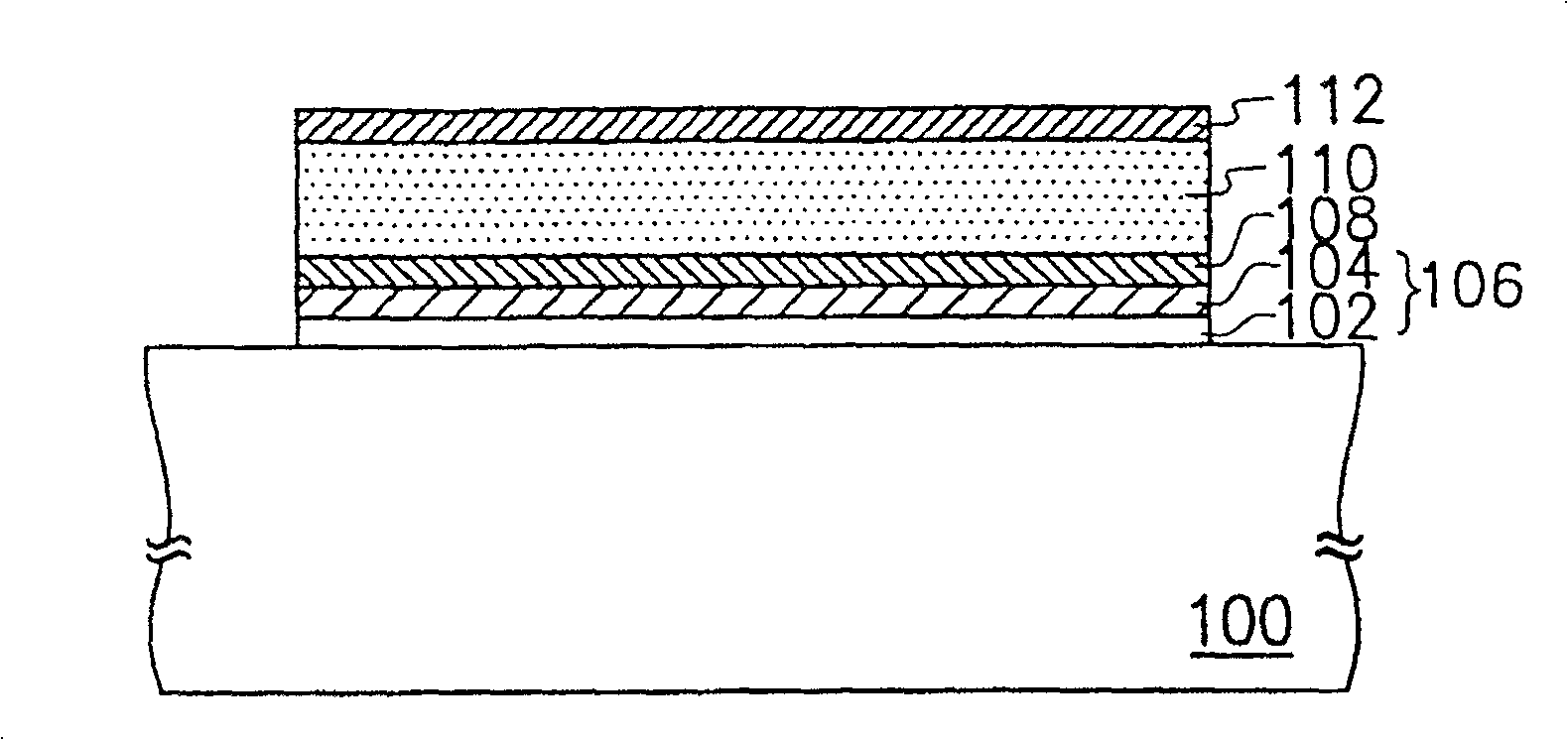
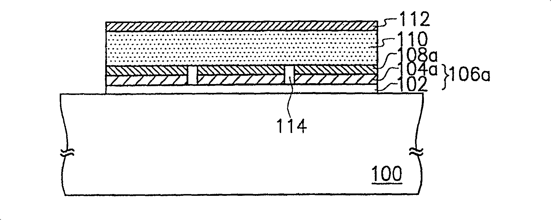
[0034] figure 1 , which is a schematic cross-sectional view of a planar light-emitting device according to a first embodiment of the present invention.

[0035] Please refer to figure 1 , the manufacturing process of the planar light-emitting device of this embodiment is to firstly provide a transparent substrate 100, wherein the transparent substrate 100 can be a plastic substrate or a bendable substrate. Afterwards, a dielectric material layer 102 is formed on the transparent substrate 100 , and a semitransparent metal layer 104 is formed on the dielectric material layer 102 , wherein the dielectric material layer 102 and the semitransparent metal layer 104 form a half lens structure 106 .

[0036] In this embodiment, the method of forming the dielectric material layer 102 is formed by physical vapor deposition or chemical vapor deposition, wherein the physical vapor deposition is, for example, sputtering, evaporation or ion plating. . The material of the dielectric mater...

no. 2 example

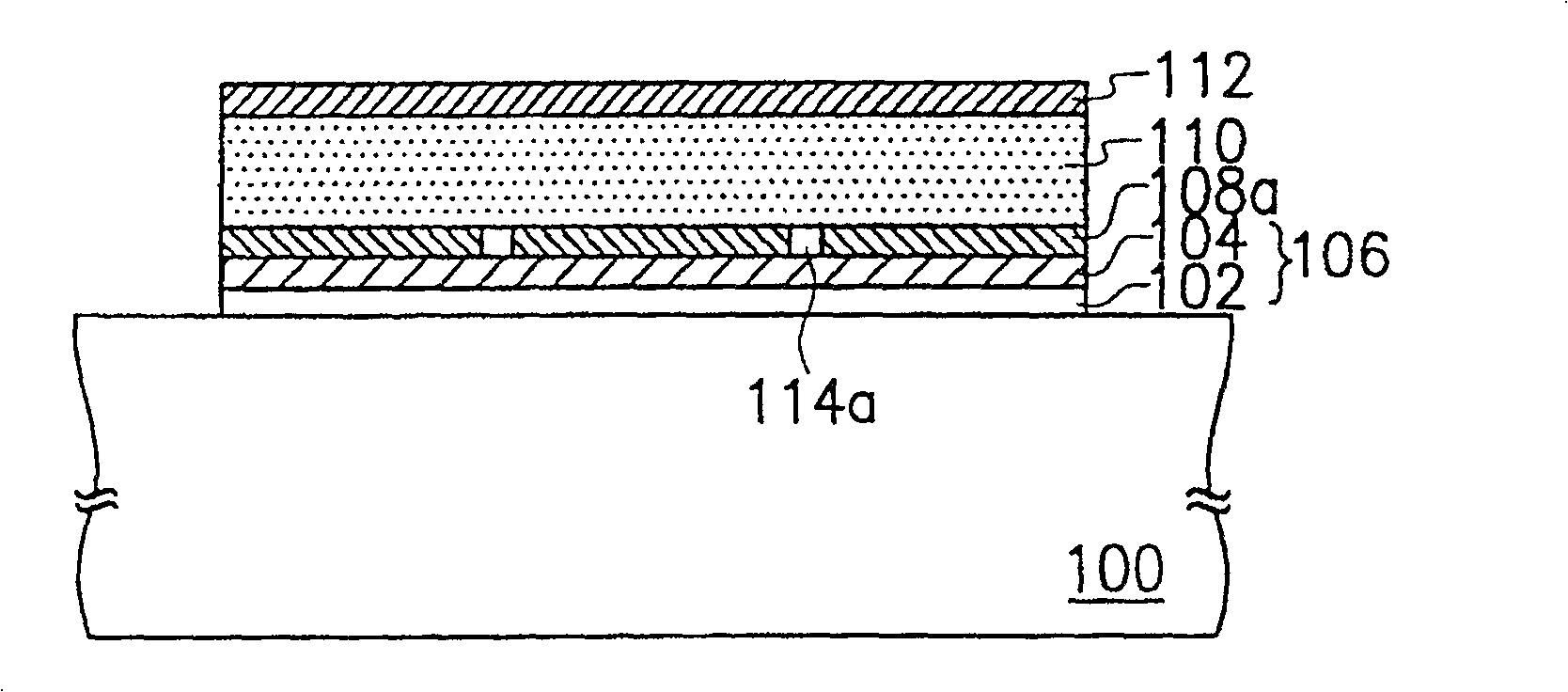
[0051] Figure 7 , which is a schematic cross-sectional view of a planar light-emitting device according to a second embodiment of the present invention.

[0052] Please refer to Figure 7 , the manufacturing process of the planar light-emitting device of this embodiment is to firstly provide a transparent substrate 100, wherein the transparent substrate 100 can be a plastic transparent substrate or a bendable transparent substrate. After that, a dielectric material layer 102 is formed on the transparent substrate 100, and a semi-transparent metal layer 104 is formed on the dielectric material layer 102, wherein the semi-transparent metal layer 104 is used as an anode, and the dielectric material layer 102 and the The semi-transparent metal layer simultaneously constitutes the half-lens structure 106 .

[0053] Here, the methods for forming the dielectric material layer 102 and the semi-transparent metal layer 104 as well as their materials and thicknesses have been describe...


PUM

PropertyMeasurementUnit
thicknessaaaaaaaaaa
thicknessaaaaaaaaaa
thicknessaaaaaaaaaa

Abstract

A planar light-emitting element and its manufacturing method. The element includes a transparent substrate; a dielectric material layer configured on the transparent substrate; a semi-transparent metal layer configured on the dielectric material layer, wherein the dielectric material layer and the semi-transparent The transparent metal layer constitutes a half-lens structure; a transparent anode is arranged on the semi-transparent metal layer; a light-emitting layer is arranged on the transparent anode; and a metal cathode is arranged on the light-emitting layer.

Description

technical field [0001] The present invention relates to a flat panel lighting device (Flat Panel Lighting Device) and a manufacturing method thereof, and in particular to a flat panel lighting device with a metal microcavity structure and a manufacturing method thereof. Background technique [0002] Among all kinds of materials that can emit light by themselves, organic electroluminescent materials are one of the most promising materials developed in recent years. The organic electroluminescent element is one of the planar light emitting elements, which not only has the advantages of simple process structure and low driving voltage, but more importantly, it can be used in plastic (Rigid Plastic) in addition to glass substrates. ) substrate and flexible (Flexible) substrate, so the organic electroluminescent element can be more widely used in optoelectronic products. [0003] For all light-emitting elements used in lighting, in addition to the requirements of high brightness...

Claims


Application Information

Patent Timeline
Patent Type & Authority Patents(China)
IPC IPC(8): H01L51/52H05B33/28H05B33/10H05B33/14
Inventor 蔡永诚魏茂国王锡九
Owner RITDISPLAY
Why Eureka
Try Eureka