

Semiconductor chip automatic centering mechanism
An alignment mechanism and automatic alignment technology, applied in semiconductor/solid-state device manufacturing, electrical components, circuits, etc., can solve problems such as wafer difficulty, and achieve the effect of reducing errors and accurate positioning
- Summary
- Abstract
- Description
- Claims
- Application Information
AI Technical Summary
Problems solved by technology
Method used
Image

Examples
Embodiment Construction
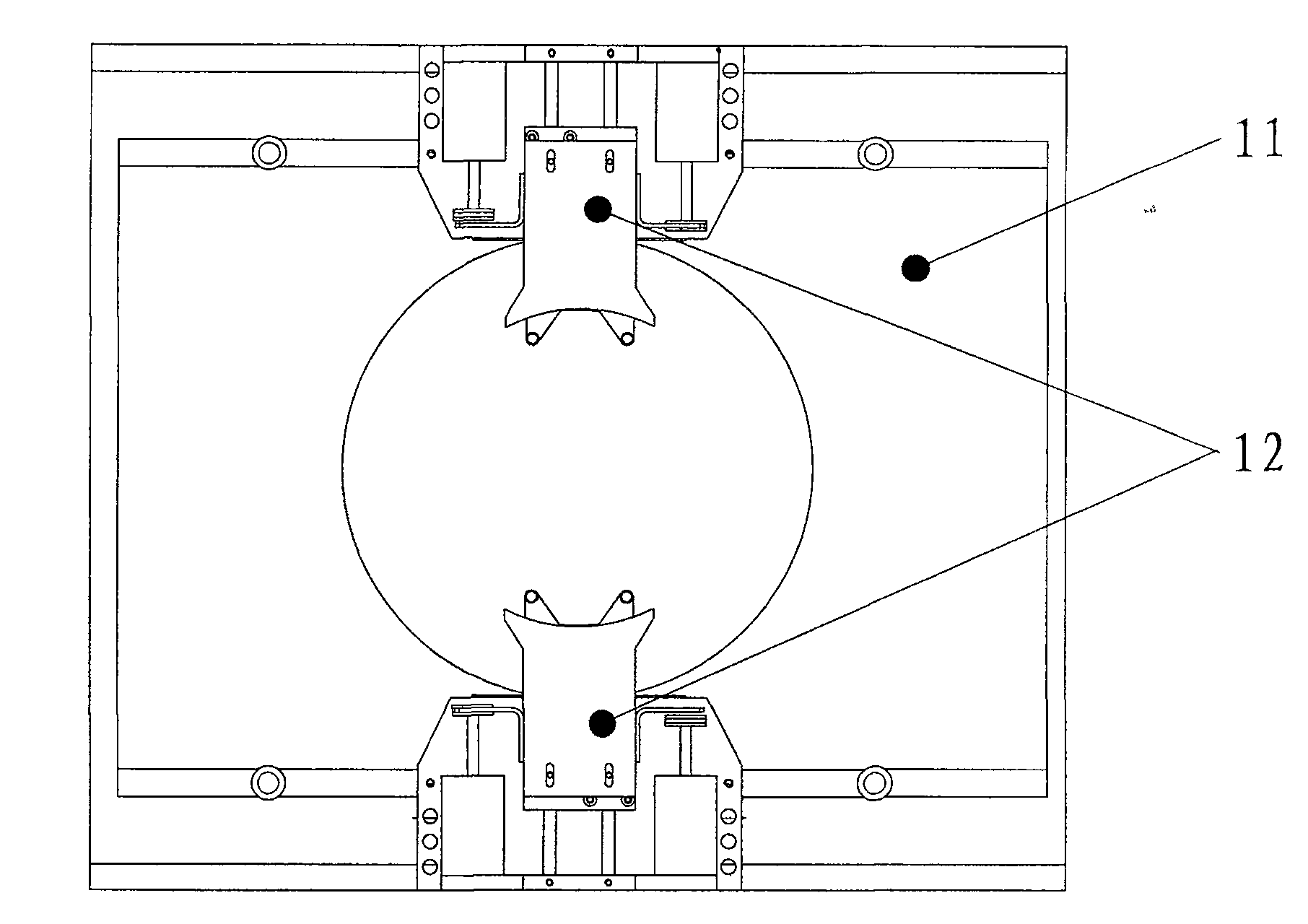
[0019] like figure 1 As shown, two centering mechanisms 12 (that is, the present invention) form a group, which are respectively installed on both sides of the wafer processing unit 11. When the wafer is transported to the central position of the wafer processing unit, the two centering mechanisms move synchronously to complete the alignment. Wafer centering action. The centering process is divided into two steps: splicing and centering. The centering mechanism can exchange the size of the centering block and the splicing plate according to the size of the processed wafer.
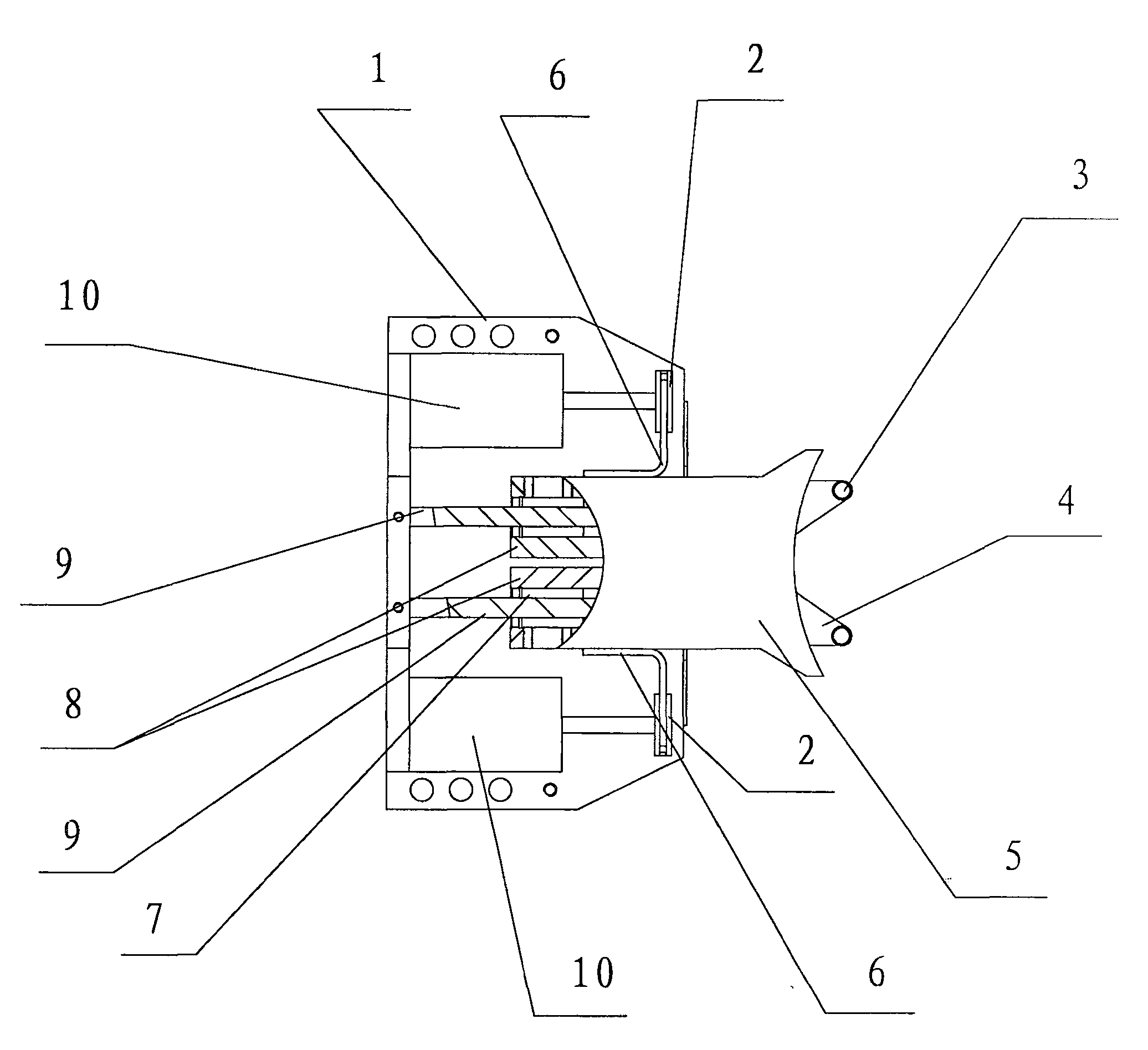
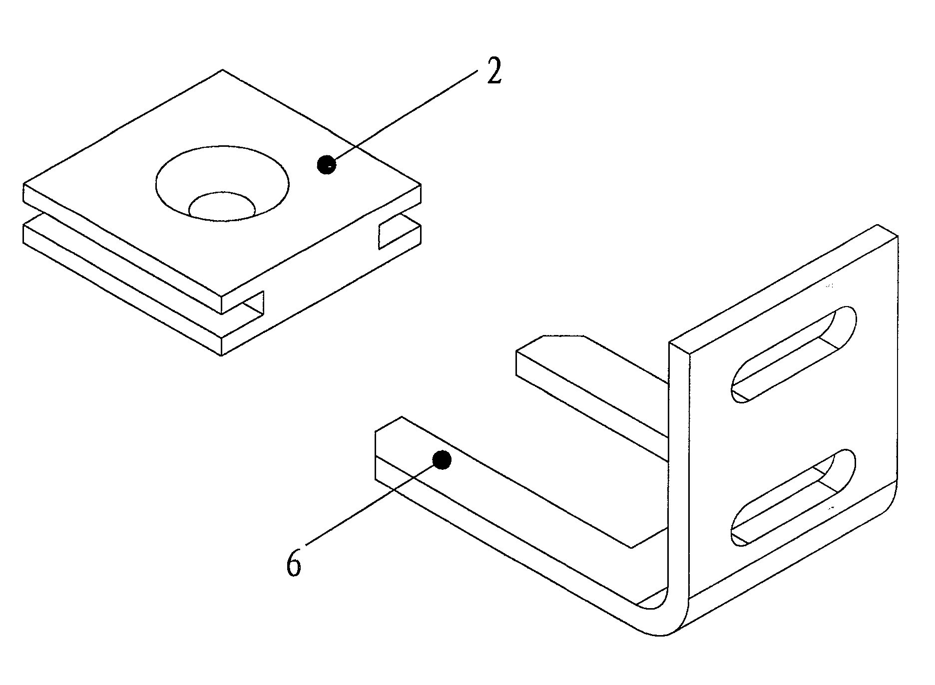
[0020] like figure 2 As shown, the centering mechanism of the present invention is provided with a bottom plate 1, a fixed block 2, a pillar 3, a joint plate 4, a centering block 5, a connecting plate 6, a linear bearing 7, a bearing seat 8, a guide rod 9, a cylinder 10, etc. The two cylinders 10 are directly fixed on the bottom plate 1, the joint plate 4 is fixed on one bearing seat 8 by screws, and th...
PUM
 Abstract
Description
Claims
Application Information