Photoelectric transducer and display panel having the same
一种光电转换装置、光电转换部的技术,应用在辨认装置、辐射控制装置、电路等方向,能够解决不能识别外部光等问题
- Summary
- Abstract
- Description
- Claims
- Application Information
AI Technical Summary
Problems solved by technology
Method used
Image

Examples
no. 1 Embodiment approach
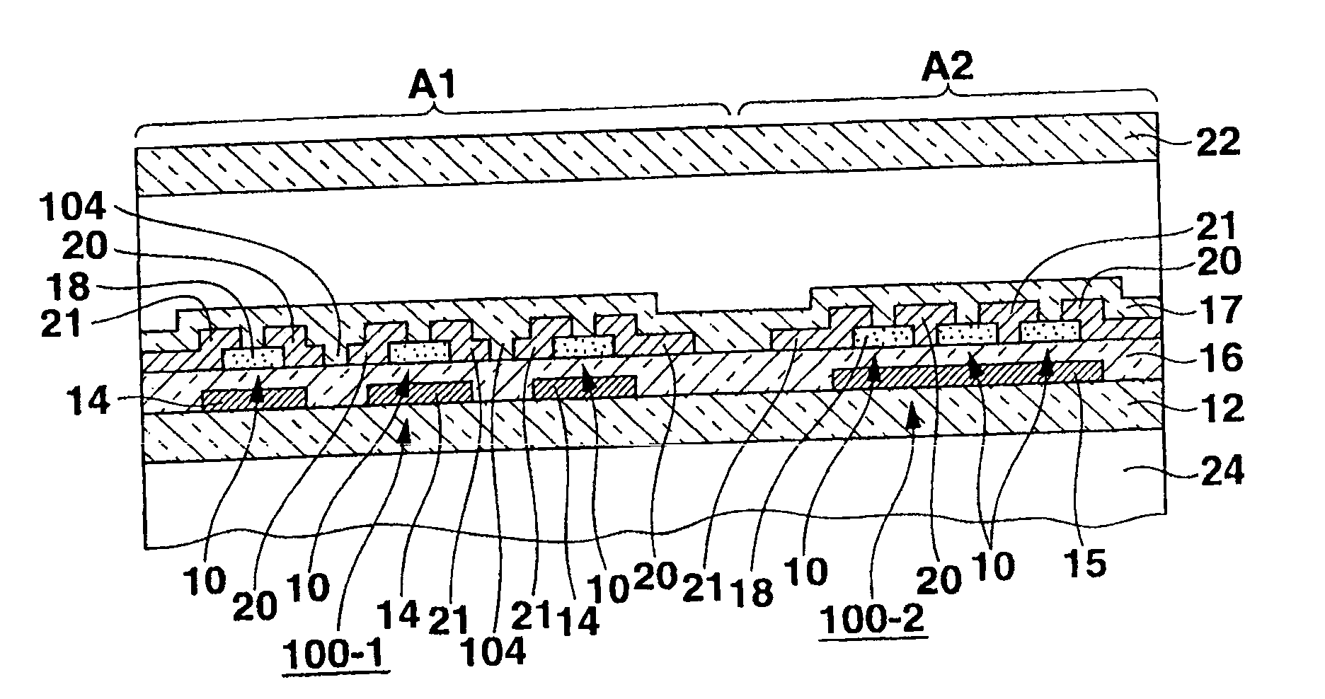
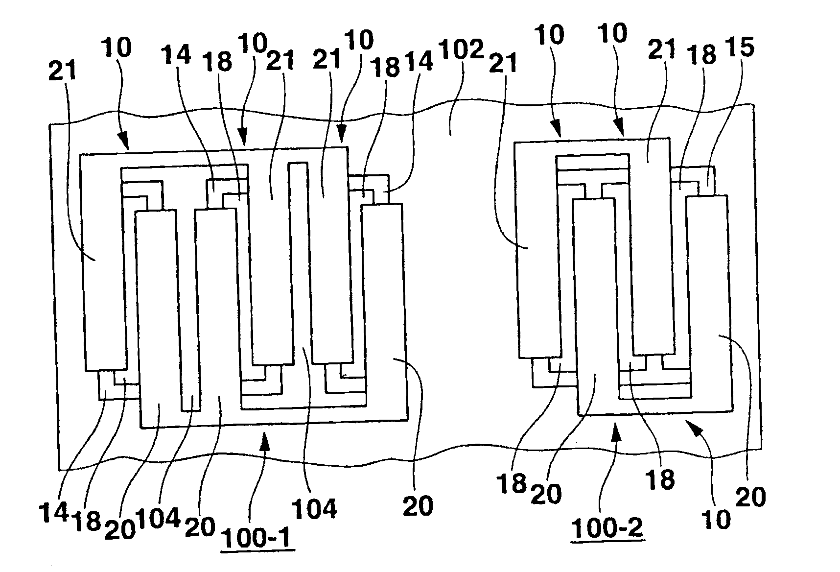
[0029] Figure 1A and Figure 1B A cross-sectional view and a plan view respectively showing the photoelectric conversion device as the first embodiment of the present invention.
[0030] This photoelectric conversion device has a first area A1 and a second area A2, in which the first sensor TFT 100-1 as the first photoelectric conversion element is arranged, and in the second area A2, the first sensor TFT 100-1 is arranged as the second photoelectric conversion element. The second sensor TFT100-2. In FIG. 1 , each of the first area A1 and the second area A2 is shown, but the first area A1 and the second area A2 are alternately arranged vertically and horizontally with a predetermined width of the inter-sensor area 102 therebetween, and constitute a photoelectric conversion element array. In addition, for the same content as the prior art, the Figure 9 same reference symbols.
[0031] The first sensor TFT 100-1 and the second sensor TFT 100-2 described above are each con...
no. 2 Embodiment approach
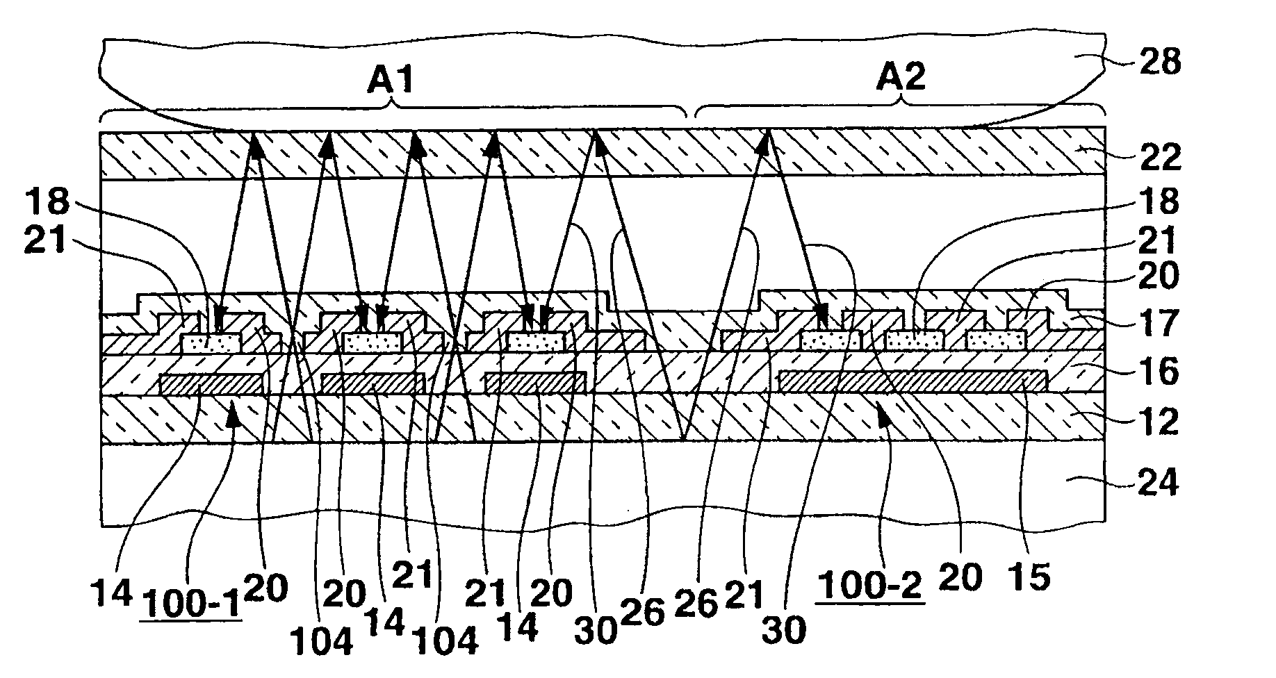
[0065] Image 6 A cross-sectional view of a photoelectric conversion device as a second embodiment of the present invention is shown. In addition, in the photoelectric conversion device of the present embodiment, the same reference numerals are assigned to the same parts as those of the photoelectric conversion device of the above-described first embodiment, and the description thereof will be omitted. In addition, only a pair of photoelectric conversion elements are shown for simplification of the drawing.
[0066] The photoelectric conversion device of the second embodiment includes first and second DG type TFT sensors 130-1 and 130-2 as the first and second sensor TFTs 130-1 and 130-2 in place of the first and second sensor TFTs 100-1 and 100-2 of the first embodiment. The first and second photoelectric conversion elements, the first and second DG type TFT sensors 130 - 1 and 130 - 2 use a double gate type amorphous silicon TFT as the TFT type photoelectric conversion elem...
no. 3 Embodiment approach
[0070] Figure 7A It is a plan view showing the structure of a photoelectric conversion device according to a third embodiment of the present invention. In this case, the photoelectric conversion device is configured such that the first area A1 in which the first sensor TFT 100-1 is disposed has five areas, and the second area A2 in which the second sensor TFT 100-2 is disposed has four areas, for the sake of simplification of the drawing. Instead, only the configuration of the gate electrodes 14 and 15 is shown. 7b is a diagram showing its circuit configuration, Figure 7C represents the equivalent circuit.
[0071] In this embodiment, as Figure 7AAs shown, the first sensor TFT 100-1 arranged in the first area A1 consists of 13 small-sized TFT photoelectric conversion elements 10 arranged in a checkered pattern, and the second sensor TFT 100-2 arranged in the second area A2 consists of 1 A large-sized TFT-type photoelectric conversion element 10 is formed. Here, the TFT...
PUM
| Property | Measurement | Unit |
|---|---|---|
| visible light transmittance | aaaaa | aaaaa |
| visible light transmittance | aaaaa | aaaaa |
Abstract
Description
Claims
Application Information
 - R&D
- Intellectual Property
- Life Sciences
- Materials
- Tech Scout
- Unparalleled Data Quality
- Higher Quality Content
- 60% Fewer Hallucinations
Browse by: Latest US Patents, China's latest patents, Technical Efficacy Thesaurus, Application Domain, Technology Topic, Popular Technical Reports.
© 2025 PatSnap. All rights reserved.Legal|Privacy policy|Modern Slavery Act Transparency Statement|Sitemap|About US| Contact US: help@patsnap.com