Prepositive differential amplifier and method for expanding its input range
A pre-differential, input range technology, applied in the direction of differential amplifiers, DC-coupled DC amplifiers, analog-to-digital converters, etc., can solve the problems of loss of dynamic range, inability to share differential mode signal amplification, and degradation of amplifier speed performance. To achieve the effect of large dynamic range
- Summary
- Abstract
- Description
- Claims
- Application Information
AI Technical Summary
Problems solved by technology
Method used
Image
Examples
Embodiment 1
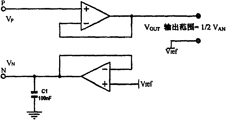
[0027] The invention provides a method for extending the input range of the pre-differential amplifier. In the method, the pre-differential amplifier can be set in a balanced input mode and an unbalanced input mode by switching. It provides a wide input range and high impedance amplifier solution for the front-end amplifier design of electronic measuring instruments. For this purpose, the output of one end of the high-impedance buffer of the differential input is reversed and then fed forward to the other end (one end can be positive or negative), or the output of the differential-mode voltage of the high-impedance buffer - 1 / 2 feed forward to the inverting input. At the same time, a DC bias voltage can also be added during the reverse amplification to shift the midpoint potential of the voltage signals output by the forward input buffer amplifier and the reverse input buffer amplifier.
Embodiment 2
[0029] The invention provides a pre-differential amplifier, which can be set to a balanced input mode and an unbalanced input mode by switching the differential amplifier. It provides a wide input range and high impedance amplifier solution for the front-end amplifier design of electronic measuring instruments. For this purpose, the output of one end of the high-impedance buffer of the differential input is reversed and then fed forward to the other end (one end can be positive or negative), or the output of the differential-mode voltage of the high-impedance buffer - 1 / 2 feed forward to the inverting input. At the same time, a DC bias voltage can also be added during the reverse amplification to shift the midpoint potential of the voltage signals output by the forward input buffer amplifier and the reverse input buffer amplifier.
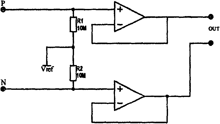
[0030] Such as figure 2 As shown, it is the circuit form of Embodiment 1 of the present invention: U1 and U2 are input buffer amplifiers, which...
Embodiment 3
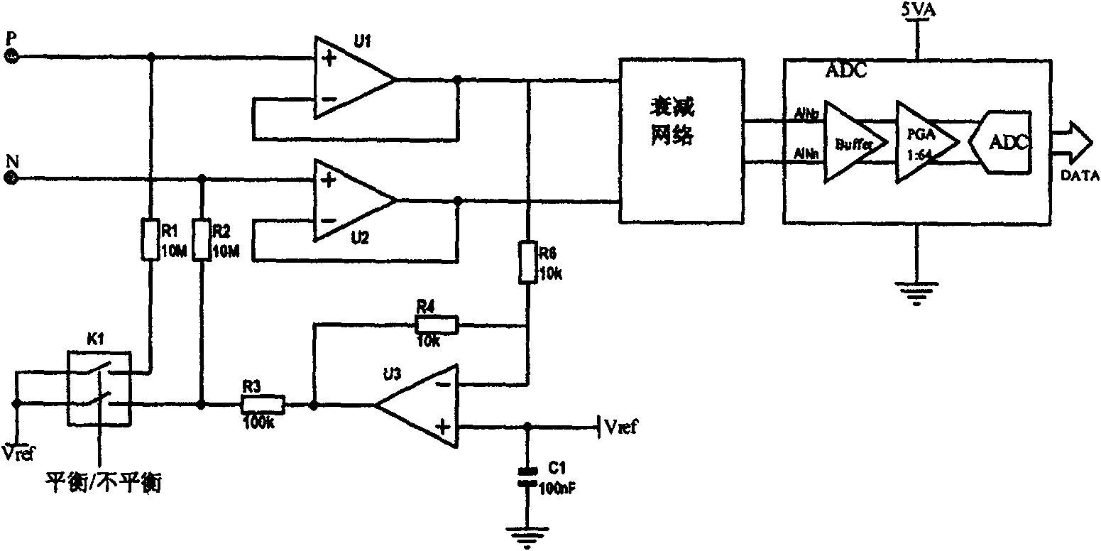
[0033] Such as image 3 As shown, it is the circuit form of Embodiment 3 of the present invention: U1 and U2 are input buffer amplifiers, which adopt CMOS or JFET structure high-voltage zero-drift operational amplifiers. image 3 In this circuit, the input buffer has a gain of 1. The connection form of the output feed-forward amplifier U3 is as follows image 3 shown. image 3 In the middle, the differential mode signal output by the buffer is attenuated by G=-1 / 2 and then fed back to the input terminal of U2. Under normal working conditions, figure 2 and image 3 The feedback amount of these two connection methods is the same, and the DC operating point is also the same, but the suppression performance of common mode noise is different. At the same time, U3 assumes the role of voltage translation, raising the midpoint potential (VP+VN) / 2 of VP and VN to VREF.
[0034] The signal after the buffer is connected to an attenuation network to ensure that the large signal doe...
PUM
 Abstract
Description
Claims
Application Information


