Non-volatile memory device, and manufacturing method and programming method thereof

A technology of non-volatile storage and manufacturing method, applied in the field of non-volatile storage devices

Inactive Publication Date: 2007-07-25
SK HYNIX INC
View PDF2 Cites 6 Cited by
  • Summary
  • Abstract
  • Description
  • Claims
  • Application Information

AI Technical Summary

Problems solved by technology

Due to the capacitive coupling of the parasitic capacitor C100, the threshold voltage Vth will vary even in the selection transistor and the memory cell, so this will create certain problems

Method used


Image

  • Non-volatile memory device, and manufacturing method and programming method thereof
  • Non-volatile memory device, and manufacturing method and programming method thereof
  • Non-volatile memory device, and manufacturing method and programming method thereof

Examples


Embodiment Construction

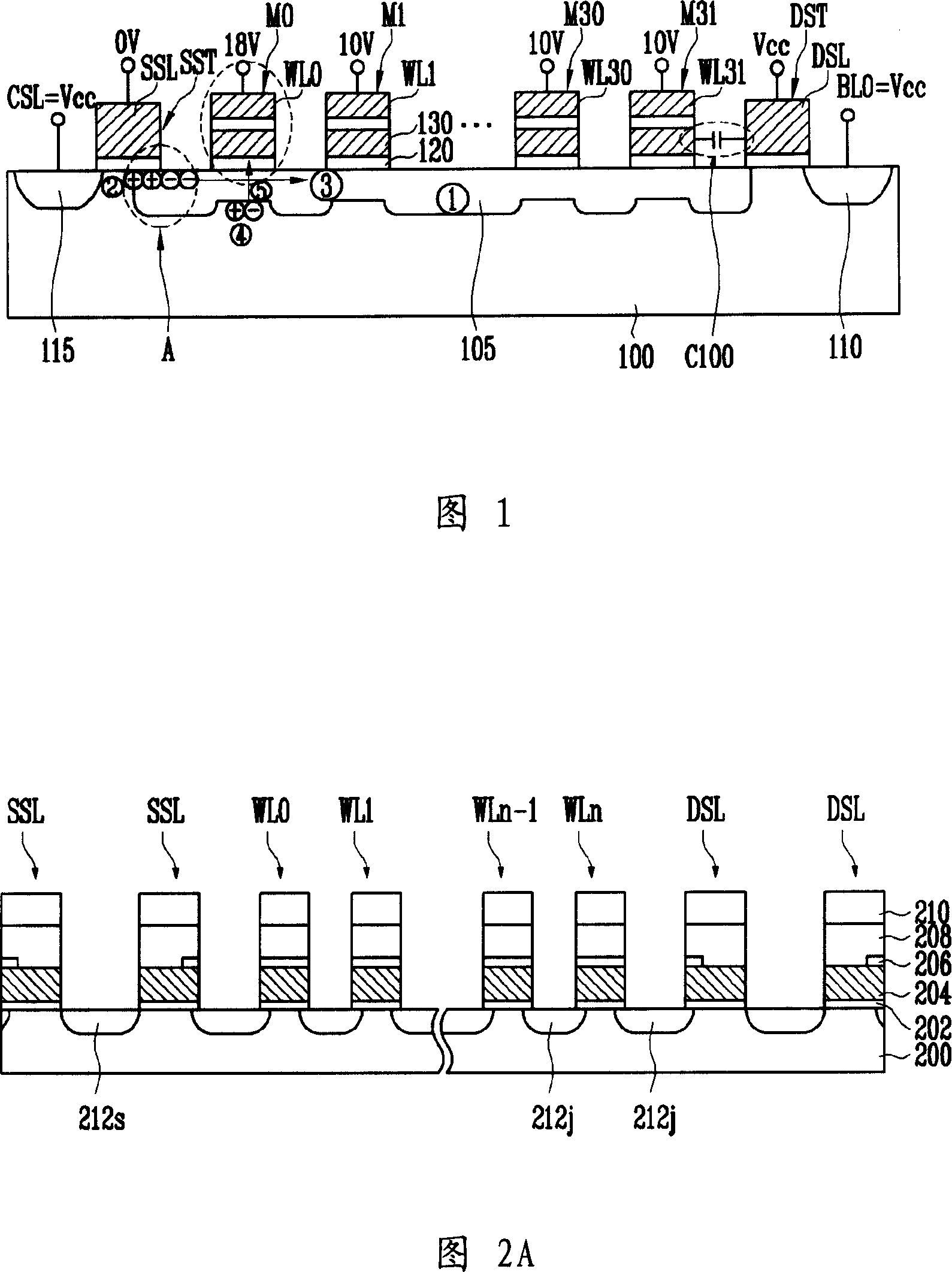
[0029] Now, specific embodiments according to the present invention will be described with reference to the accompanying drawings.

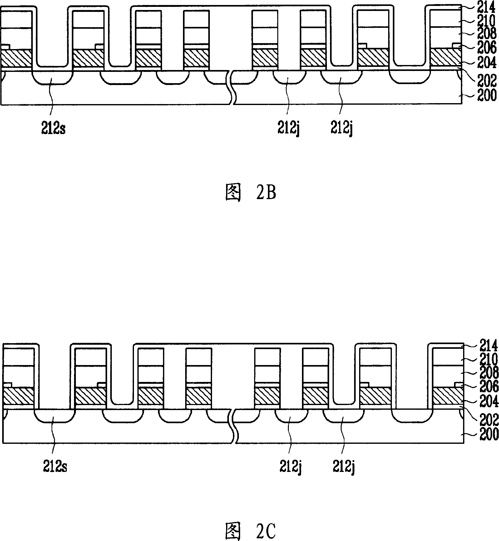
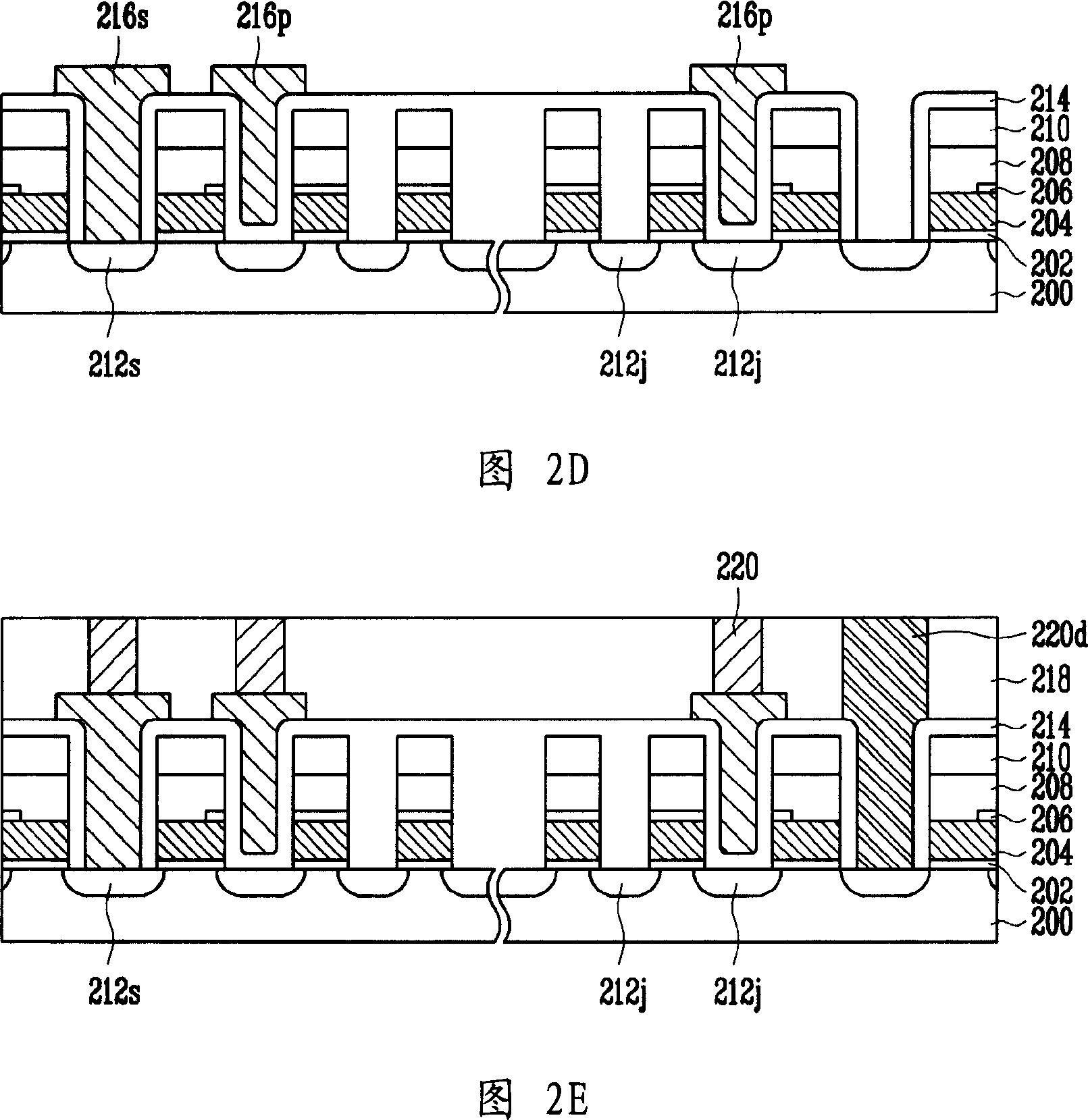
[0030] 2A to 2E are cross-sectional views illustrating a method of manufacturing a nonvolatile memory device according to an embodiment of the present invention.

[0031] Referring to FIG. 2A , a plurality of selection lines DSL and SSL and word lines WL0 to WLn are formed on a semiconductor substrate 100 . A junction region 212j, a drain 212d, and a source 212s are formed between the select line and the word line. More specifically, a plurality of word lines WL0 and WLn are formed between the drain selection line DSL and the source selection line SSL. A drain 212d to be connected to a bit line is formed in the semiconductor substrate 200 between the drain selection lines DSL, and a source 212s is formed in the semiconductor substrate 200 between the source selection lines SSL.

[0032] Meanwhile, each of the selection lines DSL and SSL and the...


PUM


Abstract

This invention discloses a non-volatile memory device, producing and programm method thereof. A non-volatile memory device includes a plurality of select lines and a plurality of word lines formed over a semiconductor substrate, a contact plug formed between the select lines, and a conductive interference shielding line formed between the select line and a word line adjacent to the select line and isolated from the semiconductor substrate.

Description

technical field [0001] The present invention generally relates to a nonvolatile memory device, and more particularly, to a nonvolatile memory device, a method of manufacturing the same, and a programming method thereof, wherein the threshold bias voltage of an unprogrammed memory cell ( bias) can be minimized. Background technique [0002] A nonvolatile memory device has a characteristic that stored data will not be erased even if power is turned off. Typical non-volatile storage devices include flash memory devices. Flash memory devices may be classified into NOR flash memory devices and NAND flash memory devices according to the structure of a memory cell array. [0003] Among them, the NAND flash memory device includes a memory cell array as a basic module unit. Each module has multiple strings. A string includes select transistors and memory cells. In more detail, the string includes a drain selection transistor connected to a bit line, a source selection transistor...

Claims


Application Information

Patent Timeline
IPC IPC(8): H01L27/115H01L23/522H01L23/552H01L21/8247H01L21/768G11C16/02G11C16/10
CPCH10B41/30
Inventor 吴尚炫安正烈权日荣
Owner SK HYNIX INC
Why Eureka
Try Eureka