Display device and electronic equipment equipped with the display device
一种显示装置、电路的技术,应用在照明装置、电光源、电气元件等方向,能够解决电容值高、耗电量增加等问题,达到提高灰度数、抑制驱动频率、抑制伪轮廓的产生的效果
- Summary
- Abstract
- Description
- Claims
- Application Information
AI Technical Summary
Problems solved by technology
Method used
Image

Examples
Embodiment approach
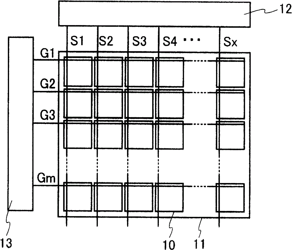
[0062] refer to Figure 1A and 1B The specific structure of the scanning line driving circuit of the present invention will be described in detail. The outline of a display device including the scanning line driving circuit of the present invention is described below.
[0063] Figure 1A The configuration of a display device including the scanning line driving circuit of the present invention is shown. Figure 1A The shown display device includes a pixel unit 11 in which a plurality of pixels 10 are formed, a signal line driver circuit 12 , and a scan line driver circuit 13 . Each of the scan lines G1 to Gm, that is, the pixels 10 of each row can be selected by the scan line drive circuit 13 . The signal line driving circuit 12 can control video signals input to the pixels 10 of the row selected by the scanning line driving circuit 13 through the signal lines S1 to Sx.
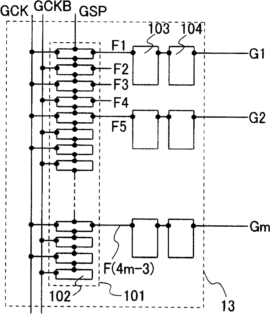
[0064] Next, refer to Figure 1B illustrate Figure 1A The structure of the scanning line driving ci...
Embodiment 1
[0079] In this example, the structure of the pixel of the display device described in the embodiment mode will be described in detail.
[0080] refer to Figure 3A to Figure 5The configuration of the display device will be described. A pixel 1010 includes a light emitting element 1013, a capacitive element 1016, and two transistors. One of the two transistors is a switching transistor 1011 (hereinafter referred to as TFT 1011 ) for controlling the input of a video signal to the pixel 1010, and the other is a driving transistor 1012 for controlling lighting and non-lighting of the light emitting element 1013. (hereinafter referred to as TFT1012). Both TFTs 1011 and 1012 are field effect transistors having three terminals of a gate electrode, a source electrode and a drain electrode.
[0081] The gate electrode of the TFT 1011 is connected to the gate line Gy, and one of the source electrode and the drain electrode thereof is connected to the source line Sx, and the other is ...
Embodiment 2
[0098] In this embodiment, referring to the timing chart ( Figure 6A ) and the timing diagram of the i-th gate line Gi (1≤i≤m) ( Figure 6B ), to describe the operation of the display device having the pixels shown in Embodiment 1. Regarding the time grayscale method, one frame period includes a plurality of subframe periods SF1, SF2, . . . , SFn (n is a natural number).
[0099]Each of the plurality of subframe periods includes one of a plurality of writing periods Ta1, Ta2, . . . ..., one of Tsn. Each of the plurality of writing periods includes a plurality of gate selection periods. Each of the plurality of gate selection periods includes a plurality of sub-gate selection periods. The number of divisions per gate selection period is not particularly limited, however, it is preferably 2 to 8, more preferably 2 to 4. In addition, the ratio of the lengths of the lighting periods Ts1:Ts2:...:Tsn is set to, for example, 2. (n-1) : 2 (n-2) :...:2 1 : 2 0 . In other wor...
PUM
 Abstract
Description
Claims
Application Information