Method for preparing power-micro structure LED tube core utilizing flip chip technology

A light-emitting diode, power-type technology, applied in the direction of electrical components, circuits, semiconductor devices, etc., can solve the problems of poor uniformity of current expansion, sacrifice of active area, and inability to realize n-electrode interconnection, etc., and achieve the effect of improving extraction efficiency

Inactive Publication Date: 2007-08-29
INST OF SEMICONDUCTORS - CHINESE ACAD OF SCI
View PDF0 Cites 21 Cited by
  • Summary
  • Abstract
  • Description
  • Claims
  • Application Information

AI Technical Summary

Problems solved by technology

At present, the production of micro-structure light-emitting diodes mainly adopts the positive structure, and it is difficult to realize the interconnection of P electrodes. Generally, microporous structures are made, but this structure cannot realize the interconnection of n electrodes, and the uniformity of current expansion is relatively poor. The turn-on voltage of the device is also relatively high
The microstructure light-emitting diodes used in microdisplays generally use horizontal and vertical wiring to realize the interconnection of p and n electrodes respectively, but the width of the electrode connection is only about ten microns, and the length is close to 1mm. In order to avoid blocking and absorbing light , the electrode should not be too thick, so the lead resistance is relatively large, and the reliability is relatively poor
In addition, this wiring method needs to reserve a large area of ​​solder joints on the chip, sacrificing a large area of ​​active area, and is not suitable for making power-type light-emitting diodes.

Method used


Image

  • Method for preparing power-micro structure LED tube core utilizing flip chip technology
  • Method for preparing power-micro structure LED tube core utilizing flip chip technology
  • Method for preparing power-micro structure LED tube core utilizing flip chip technology

Examples


Embodiment

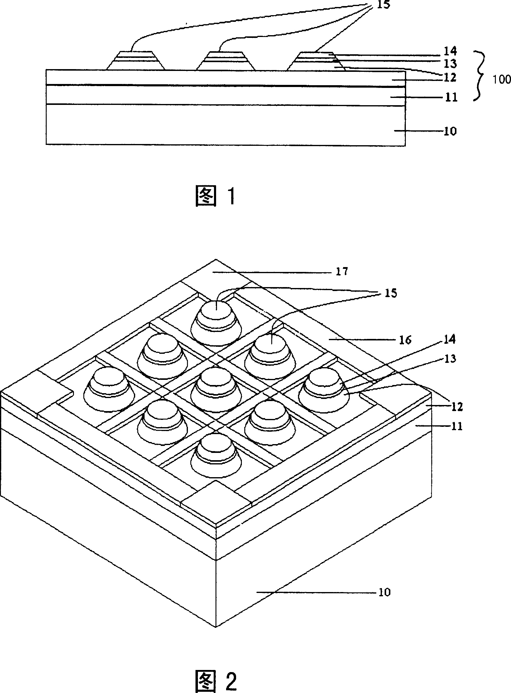
[0047]First, please refer to FIG. 1 , which is a cross-sectional view of a flip-chip microstructure GaN-based light-emitting diode die structure after the dry etching process is completed. The manufacturing process is to epitaxially grow a GaN or AlGaN buffer layer 11, an n-type GaN layer 12, an active layer 13 and a p-type GaN layer 14 on a sapphire substrate 10 by MOCVD method, and the active layer structure is InGaN / GaN or AlGaN / GaN multiple quantum wells, microstructure GaN-based power light-emitting diodes. The shape of the die is designed to be square, with a size of 1mm×1mm. The microstructure is designed to have a size of 4-20μm and a center-to-center spacing of 20-50μm. Or a square platform (the present invention takes a circular platform with a diameter of 20 μm and a center distance of 50 μm as an example). This structure increases the exit area of ​​the light emitted by the active layer. Since the size is less than 20 μm, it greatly reduces the absorption of light ...


PUM

PropertyMeasurementUnit
sizeaaaaaaaaaa
thicknessaaaaaaaaaa
diameteraaaaaaaaaa

Abstract

This invention relates to a method for processing cores of power-like microstructure LED by a flip technology including the following steps: 1, growing an epitaxial layer structure on a sapphire substrate, 2, etching a round desk on the epitaxial layer structure, 3, processing n type meshed Ohm contact electrode and electrode solder points, 4, depositing SiO2 or SiN4 insulation layer on the top surface of the device structure, 5, eroding the insulation layer on the top surface of the round desk, 6, depositing p-type thickened high reflection rate metal electrode on the top surface of the device except the electrode solder points, 7, etching to erode the insulation layer on the n electrode solder points, 8, thinning the back of the sapphire substrate to cut it to single core structures, 9, depositing a medium layer on the silicon support body, 10, flip-soldering the core structure and the Si supporting body via the convex points, 11, cutting it to form a core of a LED.

Description

technical field [0001] The invention belongs to the technical field of semiconductors, and in particular refers to a method for manufacturing a power-type microstructure light-emitting diode tube core by flip-chip technology. Background technique [0002] Gallium nitride-based compound semiconductors mostly use quantum wells and heterojunction structures as the active area of ​​light-emitting diodes. This light-emitting diode has the advantages of good reliability, high efficiency, long life, and energy saving. It is used in large-screen displays, indications, and liquid crystal displays. , the field has broad application prospects, especially the combination of gallium nitride-based purple and blue light-emitting diodes with phosphors can produce visually white light-emitting diodes, which can be used for daily lighting. In order to meet the requirements of future lighting, the luminous efficiency of light-emitting diodes still needs to be further improved. The size of tra...

Claims


Application Information

Patent Timeline
Patent Type & Authority Applications(China)
IPC IPC(8): H01L33/00H01L33/48H01L33/60H01L33/62H01L33/64
Inventor 郭金霞王良臣
Owner INST OF SEMICONDUCTORS - CHINESE ACAD OF SCI
Why Eureka
Try Eureka