Nitride-based semiconductor light-emitting device and method of manufacturing the same

a technology of nitride-based semiconductors and light-emitting devices, which is applied in the direction of semiconductor devices, building locks, construction, etc., can solve the problems of high light extraction efficiency of nitride-based semiconductor leds, complicated manufacturing process, and many additional processes, so as to maximize the light extraction efficiency of leds, enhance light extraction efficiency, and improve structure

Active Publication Date: 2007-08-30
SAMSUNG ELECTRONICS CO LTD
View PDF12 Cites 82 Cited by
  • Summary
  • Abstract
  • Description
  • Claims
  • Application Information

AI Technical Summary

Benefits of technology

[0010]The present invention may provide a nitride-based semiconductor light-emitting device having an improved structure to enhance the light extraction efficiency, and a method of manufacturing the same.
[0014]According to the present invention, a nitride-based semiconductor light-emitting device having an improved structure to enhance light extraction efficiency can be provided. In particular, according to the present invention, an LED is manufactured by forming the p-contact layer, the n-contact layer and the n-electrode to have rough surfaces without additional lithography and etching processes, thereby maximizing the light extraction efficiency of the LED.

Problems solved by technology

Thus the light extraction efficiency of the nitride-based semiconductor LED is not high.
Thus, the above-proposed methods require many additional processes.
Also, in order to simultaneously obtain the three structures described above, all of the above processes must be performed, thereby complicating the manufacturing process.
Thus, the manufacturing process is complicated and the productivity is low.

Method used


Image

  • Nitride-based semiconductor light-emitting device and method of manufacturing the same
  • Nitride-based semiconductor light-emitting device and method of manufacturing the same
  • Nitride-based semiconductor light-emitting device and method of manufacturing the same

Examples


Embodiment Construction

[0023]The present invention will now be described more fully with reference to the accompanying drawings, in which exemplary embodiments of the invention are shown. In the drawings, the thicknesses of layers and regions are exaggerated for clarity.

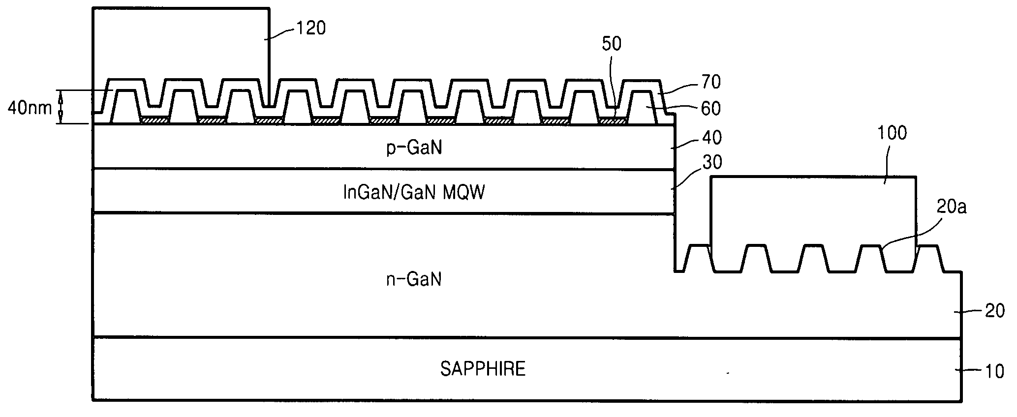
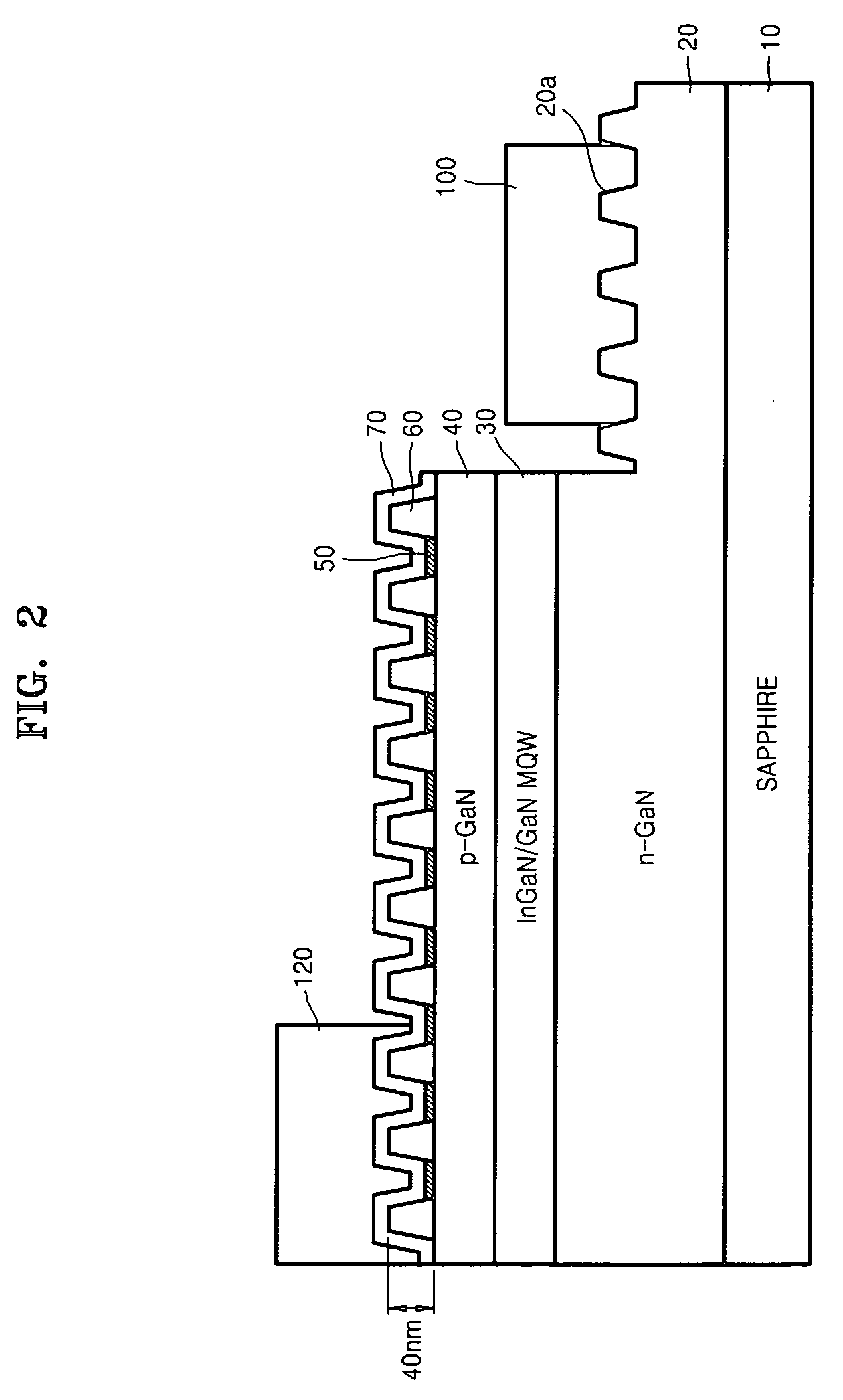
[0024]FIG. 2 is an enlarged cross-sectional view of a nitride-based semiconductor light-emitting device according to an embodiment of the present invention. FIG. 3 is a SEM photograph of the upper face of a p-contact layer of the nitride-based semiconductor light-emitting device of FIG. 2.

[0025]Referring to FIG. 2, the nitride-based semiconductor light-emitting device includes an n-clad layer 20, an active layer 30, a p-clad layer 40, a plurality of masking dots 50, and a p-contact layer 60 that are sequentially stacked on a substrate 10. The p-contact layer 60 is formed on the p-clad layer 40 between the masking dots 50 and has a rough structure. Also, an n-electrode 100 and a p-electrode 120 are formed on an etched surface 20a of the n-c...


PUM


Abstract

A nitride-based semiconductor light-emitting device having an improved structure to enhance light extraction efficiency, and a method of manufacturing the same are provided. The method includes the operations of sequentially forming an n-clad layer, an active layer, and a p-clad layer on a substrate; forming a plurality of masking dots on an upper surface of the p-clad layer; forming a p-contact layer having a rough surface on portions of the p-clad layer between the masking dots; forming a rough n-contact surface of the n-clad layer having the same rough shape as the rough shape of the p-contact layer by dry-etching from a portion of the upper surface of the p-contact layer to a desired depth of the n-clad layer; forming an n-electrode on the rough n-contact surface; and forming a p-electrode on the p-contact layer.

Description

CROSS-REFERENCE TO RELATED PATENT APPLICATION[0001]This application claims the benefit of Korean Patent Application No. 10-2006-0018445, filed on Feb. 24, 2006, in the Korean Intellectual Property Office, the disclosure of which is incorporated herein in its entirety by reference.BACKGROUND OF THE DISCLOSURE[0002]1. Field of the Disclosure[0003]The present disclosure relates to a semiconductor light-emitting device, and particularly to a nitride-based semiconductor light-emitting device having an improved structure to enhance light extraction efficiency, and a method of manufacturing the same.[0004]2. Description of the Related Art[0005]Light-emitting diodes (LED) are devices used for emitting electrical energy in the form of infrared rays, visible light, or the other light using the characteristics of compound semiconductors. A group III nitride compound semiconductor is a direct transition semiconductor. The group III nitride compound semiconductor is widely utilized in light-emit...

Claims


Application Information

Patent Timeline
Patent Type & Authority Applications(United States)
IPC IPC(8): H01L21/00H01L33/32H01L33/22
CPCH01L33/14H01L33/20H01L2933/0016H01L33/32H01L33/382H01L33/22E05B15/10
Inventor YOON, SUK-HOSONE, CHEOL-SOOLEE, JEONG-WOOKKIM, JOO-SUNG
Owner SAMSUNG ELECTRONICS CO LTD
Why Eureka
Try Eureka