

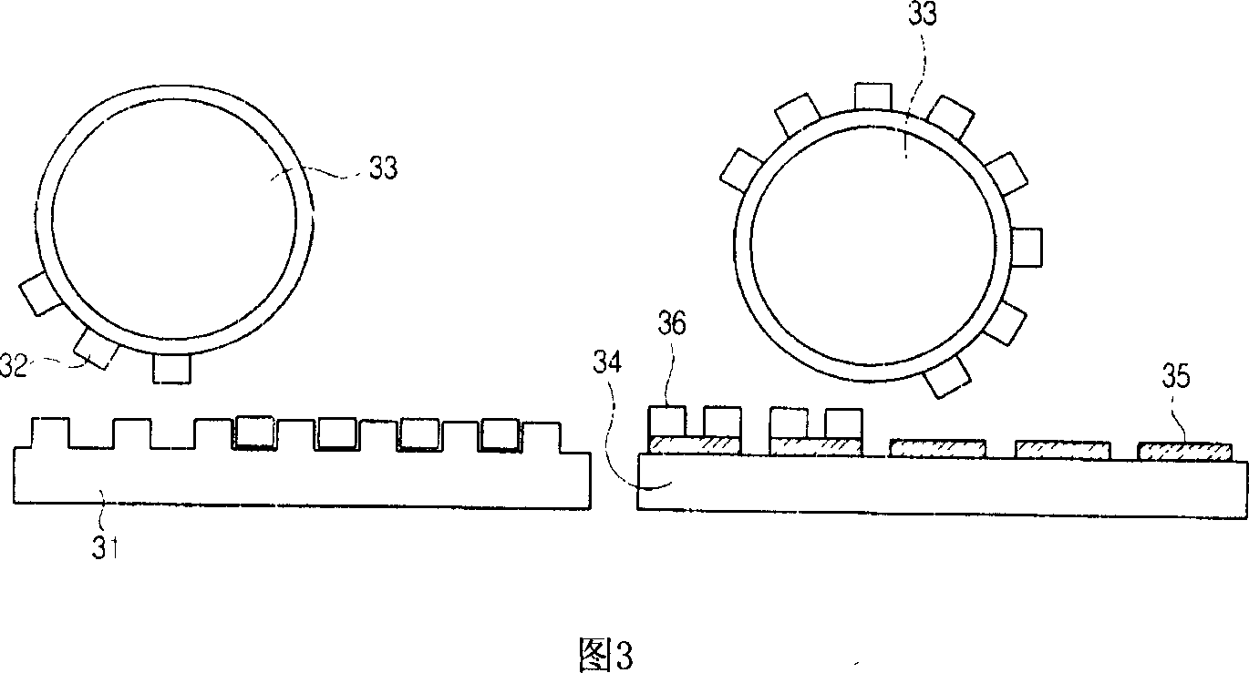
Method for making electrode of plasma display panel
A plasma display panel and electrode manufacturing technology, which is applied in the direction of alternating current plasma display panel, electrode system manufacturing, cold cathode manufacturing, etc., can solve the problems that bus electrodes 36 and black matrix 35 cannot be accurately overlapped and difficult, and achieve easy manufacturing, The effect of simplifying the manufacturing process
- Summary
- Abstract
- Description
- Claims
- Application Information
AI Technical Summary
Problems solved by technology
Method used
Image

Examples
Embodiment Construction
[0028] With reference to accompanying drawing, specifically introduce the present invention as follows:
[0029] The picture is added in order to introduce the present invention, and Fig. 4 shows the sequence diagram of the electrode manufacturing process of the plasma display panel in the example of the present invention, and Fig. 5a to Fig. 5d show the sequence section for introducing the electrode manufacturing process shown in Fig. 4 picture.
[0030] Taking the above picture as a reference, the manufacturing process of forming the black matrix and electrode structures in the example of the present invention and moving them to the upper glass substrate to simultaneously form the black matrix and bus electrodes on the upper plate of the PDP is introduced.
[0031] With reference to the sequence diagram in Fig. 4 attached above, analyzing the electrode manufacturing method of the plasma display panel in the present invention, it can be learned that: after forming the black m...
PUM
 Abstract
Description
Claims
Application Information