Method for making electrode of plasma display panel

A plasma display panel and electrode manufacturing technology, which is applied in the direction of alternating current plasma display panel, electrode system manufacturing, cold cathode manufacturing, etc., can solve the problems that bus electrodes 36 and black matrix 35 cannot be accurately overlapped and difficult, and achieve easy manufacturing, The effect of simplifying the manufacturing process

Inactive Publication Date: 2009-05-06
LG ELECTRONICS(NANJING) PLASMA CO LTD
View PDF3 Cites 0 Cited by
  • Summary
  • Abstract
  • Description
  • Claims
  • Application Information

AI Technical Summary

Problems solved by technology

Therefore, when printing the bus electrodes 36, mistakes are caused by the rotation of the blanket 33 and the movement of the upper glass substrate 34, and there is a problem that the bus electrodes 36 and the black matrix 35 cannot be accurately overlapped, but the bus electrodes 36 are formed outside the black matrix.
[0014] Different from the traditional photolithography process that undergoes complex processes after paste printing, the offset printing process has advantages in reducing material costs and simplifying the process. However, the bus electrodes 36 must be accurately overlapped on the black matrix 35, and the upper glass substrate in a wide area Form bus electrode 36 on 34, then have difficulty

Method used


Image

  • Method for making electrode of plasma display panel
  • Method for making electrode of plasma display panel
  • Method for making electrode of plasma display panel

Examples


Embodiment Construction

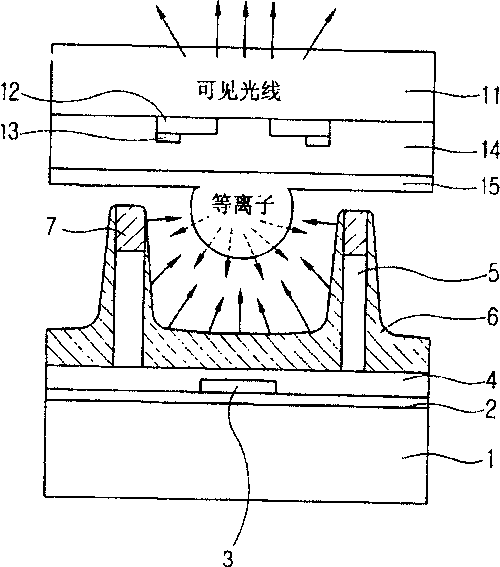
[0028] With reference to the drawings, the present invention is specifically introduced as follows:

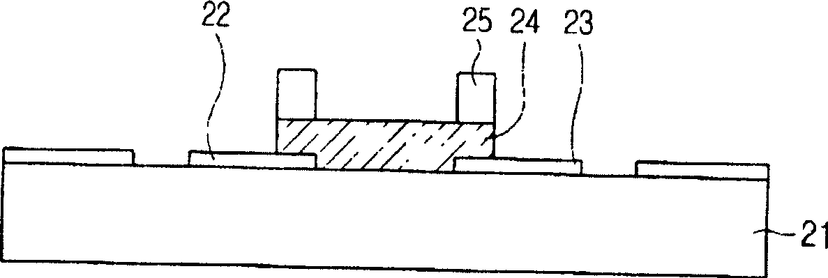
[0029] The picture is added to introduce the present invention, Figure 4 Shown is a sequence diagram of the electrode manufacturing process of the plasma display panel in the example of the present invention, Figure 5 a to Figure 5 d shows the introduction Figure 4 A sequential cross-sectional view of the electrode manufacturing process shown.

[0030] Taking the above pictures as a reference, the manufacturing process of forming the black matrix and electrode structure in the example of the present invention is introduced, and then moved to the upper glass substrate, so that the black matrix and bus electrodes are formed on the PDP upper plate at the same time.

[0031] With the above attached Figure 4 The sequence diagram is for reference. After analyzing the electrode manufacturing method of the plasma display panel of the present invention, it can be seen that after forming...


PUM


Abstract

The present invention is an invention related to the electrode manufacturing method of the plasma display panel. When the conventional technology exists to print the bus electrodes, errors are caused by the rotation and movement between the blanket and the upper glass substrate, so that the bus electrodes and the black matrix cannot be accurately overlapped. , and the problem of forming bus electrodes outside the black matrix. Considering these problems, the structure of the present invention is to set electrodes on the cathode frame and the structure of the black matrix overlapping the above electrodes, and then move the formed structure to the substrate for printing, thereby simultaneously forming the black matrix and the electrode combination structure. . Therefore, by simultaneously forming the black matrix and the bus electrodes on the upper glass substrate, the manufacturing process of the plasma display panel can be simplified, and the bus electrodes can be formed on the edge of the black matrix without dislocation between the black matrix and the bus electrodes, thereby The effect of the bus electrode of the fine model can be easily produced.

Description

Technical field [0001] The present invention is an invention related to an electrode manufacturing method of a plasma display panel, in particular, an invention related to an electrode manufacturing method of a plasma display panel that can simplify the electrode manufacturing process of the plasma display panel. Background technique [0002] Together with TFT liquid crystal display elements (LCD), organic, FED, etc., the plasma display panel (Plsama Display Panel, hereinafter referred to as PDP) element that has attracted attention as the second-generation display element is: the discharge is separated by barrier ribs. When the helium (He) + xenon (Xe) or neon (Ne) + xenon (Xe) gas discharges in the cell, 147nm ultraviolet rays are generated to excite the R, G, B phosphors, and use the phosphors to recover from the excited state to the base state It is a display element that emits light due to the difference in energy at the time. The above-mentioned PDP display elements are exp...

Claims


Application Information

Patent Timeline
Patent Type & Authority Patents(China)
IPC IPC(8): H01J9/02H01J11/20H01J11/22H01J11/44
CPCH01J9/02H01J9/2278H01J11/12H01J11/32H01J11/44H01J2211/444
Inventor 徐炳华全源锡金济奭柳炳吉
Owner LG ELECTRONICS(NANJING) PLASMA CO LTD
Why Eureka
Try Eureka