Structure of display panel for improving the static discharge resistance

A display panel and electrostatic discharge technology, applied in the direction of static electricity, static indicators, electrical equipment structural parts, etc., can solve the problems of display panel 100 damage, impact on pixel units, etc., and achieve the effect of improving electrostatic discharge resistance

Inactive Publication Date: 2007-09-12
NOVATEK MICROELECTRONICS CORP
View PDF2 Cites 12 Cited by
  • Summary
  • Abstract
  • Description
  • Claims
  • Application Information

AI Technical Summary

Problems solved by technology

However, in the conventional technology, part of the electrostatic current will still impact each pixel unit (such as the pixel unit 131) and the integrated circuit 120
If the ESD protection element 133 fails to activate immediately, the display panel 100 will still be damaged due to ESD

Method used


Image

  • Structure of display panel for improving the static discharge resistance
  • Structure of display panel for improving the static discharge resistance
  • Structure of display panel for improving the static discharge resistance

Examples


Embodiment Construction

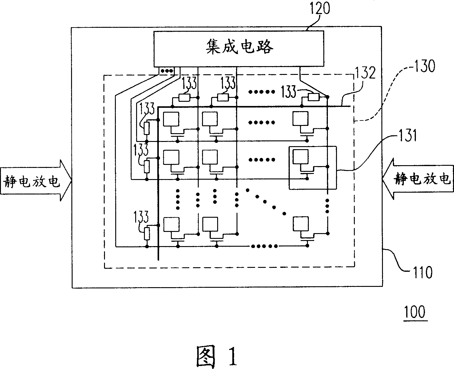
[0034] For convenience and clear description of the spirit and technical characteristics of the present invention, the liquid crystal display panel of the "chip-on-glass" technology will be used as an example below to illustrate the application of the present invention in the liquid crystal display panel (or thin film transistor) Display panel) implementation example. The scope of application of the present invention should not be limited by the teachings of the following embodiments. Those skilled in the art can apply the present invention to display panels of any type and technology according to their needs.

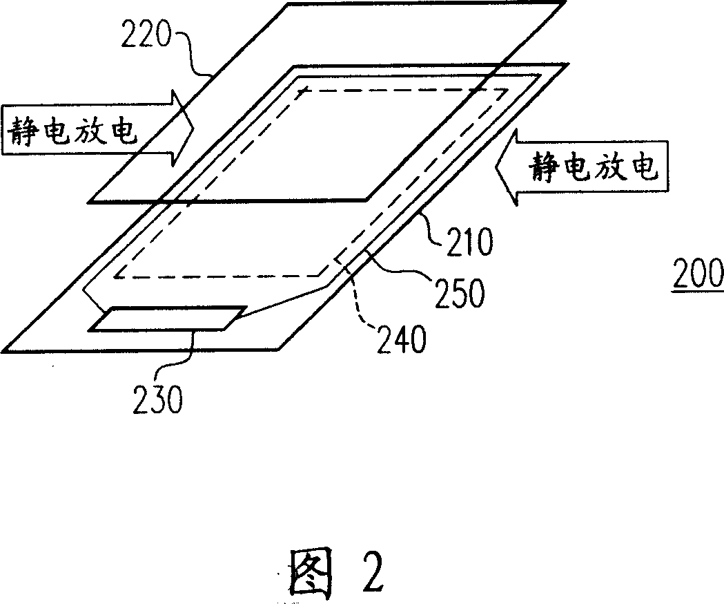
[0035] FIG. 2 illustrates an embodiment of a display panel structure for improving ESD resistance according to the present invention. The display panel 200 includes a first substrate 210 , a second substrate 220 , an integrated circuit 230 , a pixel array area 240 and an ESD protection path 250 . In this embodiment, the main materials of the substrates 210 and 220 ar...


PUM


Abstract

The invention relates to a display panel structure for improving static discharge resistance, comprising first substrate, pixel array region and static discharge protection path, where the pixel array region is arranged on the first substrate, the pixel array region is equipped with at least a pixel cell and at least a data channel, and the static discharge protection path encircles the pixel array region to conduct static current.

Description

technical field [0001] The present invention relates to an electrostatic discharge protection device, and in particular to a display panel structure for improving electrostatic discharge resistance. Background technique [0002] Electronic products are often subject to electrostatic discharge (ESD) impacts in actual use environments, and internal components will be damaged if no proper protection measures are taken. In fact, the electrostatic discharge voltage is much higher than the general power supply voltage. When the electrostatic discharge occurs, the electrostatic discharge current is likely to burn the components. So how to isolate static electricity and avoid component damage is very important. In order to avoid the aforementioned situation, some electrostatic discharge protection measures must be taken in the circuit. The International Electrotechnical Commission (IEC) has formulated several protection and testing standards for ESD immunity and electromagnetic co...

Claims


Application Information

Patent Timeline
Patent Type & Authority Applications(China)
IPC IPC(8): H05F3/02H05K7/00G02F1/133G09F9/00
Inventor 张智毅
Owner NOVATEK MICROELECTRONICS CORP
Why Eureka
Try Eureka