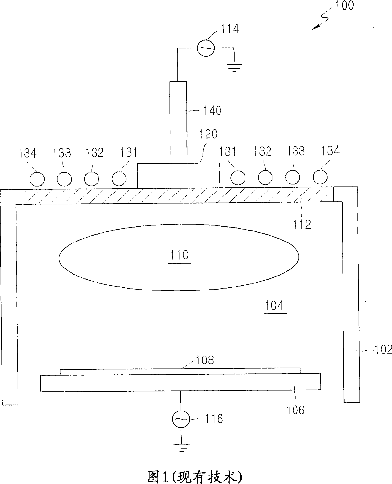
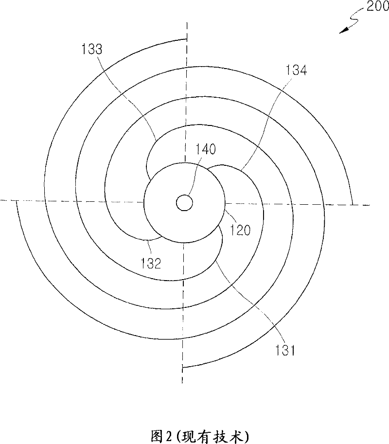
Plasma source for uniform plasma distribution in plasma chamber
A plasma source and plasma technology, applied in the field of plasma chambers, can solve the problems of magnetic field deviation, difficult to control the etching rate of critical scale, etc., and achieve the effects of preventing magnetic field deviation, enhancing selectivity, and uniform CD distribution
- Summary
- Abstract
- Description
- Claims
- Application Information
AI Technical Summary
Problems solved by technology
Method used
Image

Examples
Embodiment Construction
[0066] Preferred embodiments of the present invention will be described with reference to the accompanying drawings.
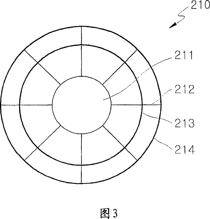
[0067] 3 is a plan view showing a plasma source according to a first embodiment of the present invention, and FIG. 4 is a cross-sectional view showing the plasma source of FIG. 3 .
[0068] Referring to FIGS. 3 and 4 , the plasma source 210 of the first embodiment includes a liner 211 , a middle source coil 213 , an edge source coil 214 , and a plurality of linear source coils 212 . The bushing 211 is formed of a conductive material, and, although not shown in the drawing, the bushing 211 is located at the upper center of the reaction chamber. The bushing 211 has a protrusion 211 - 1 at the center of the bushing 211 to transmit RF power from an external RF power source (not shown) to the bushing 211 . The linear source coil 212 extends linearly from the edge of the liner 211 to the upper edge of the reaction chamber. Since the bushing 211 is electrically con...
PUM
 Abstract
Description
Claims
Application Information
 - R&D Engineer
- R&D Manager
- IP Professional
- Industry Leading Data Capabilities
- Powerful AI technology
- Patent DNA Extraction
Browse by: Latest US Patents, China's latest patents, Technical Efficacy Thesaurus, Application Domain, Technology Topic.
© 2024 PatSnap. All rights reserved.Legal|Privacy policy|Modern Slavery Act Transparency Statement|Sitemap