Schottky part and semiconductor making process for making same

A technology for semiconductors and components, which is applied in the field of semiconductor manufacturing of Schottky components, can solve the problems of reduced ion concentration, increased conduction resistance, and increased cost, and achieves the effect of reducing cost and reducing conduction resistance.

Inactive Publication Date: 2007-10-10
SYST GEN
View PDF0 Cites 4 Cited by
  • Summary
  • Abstract
  • Description
  • Claims
  • Application Information

AI Technical Summary

Problems solved by technology

[0003] However, in order to increase the breakdown voltage in the Schottky element 1, the ion concentration in the N-type deep well region 103 will decrease
Therefore, the production of the Schottky element 1 will require many additional photomasks and processes, resulting in a relatively high cost
In addition, the conduction resistance of the Schottky element 1 will also increase relatively

Method used


Image

  • Schottky part and semiconductor making process for making same
  • Schottky part and semiconductor making process for making same
  • Schottky part and semiconductor making process for making same

Examples


no. 1 example

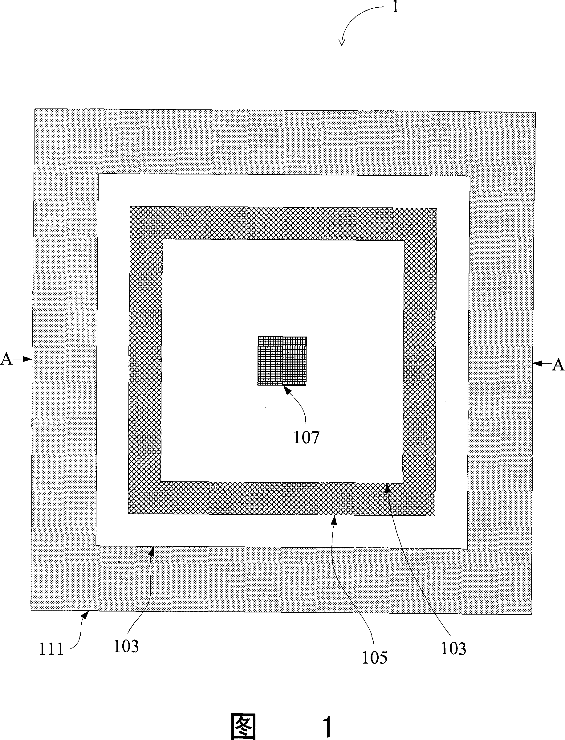
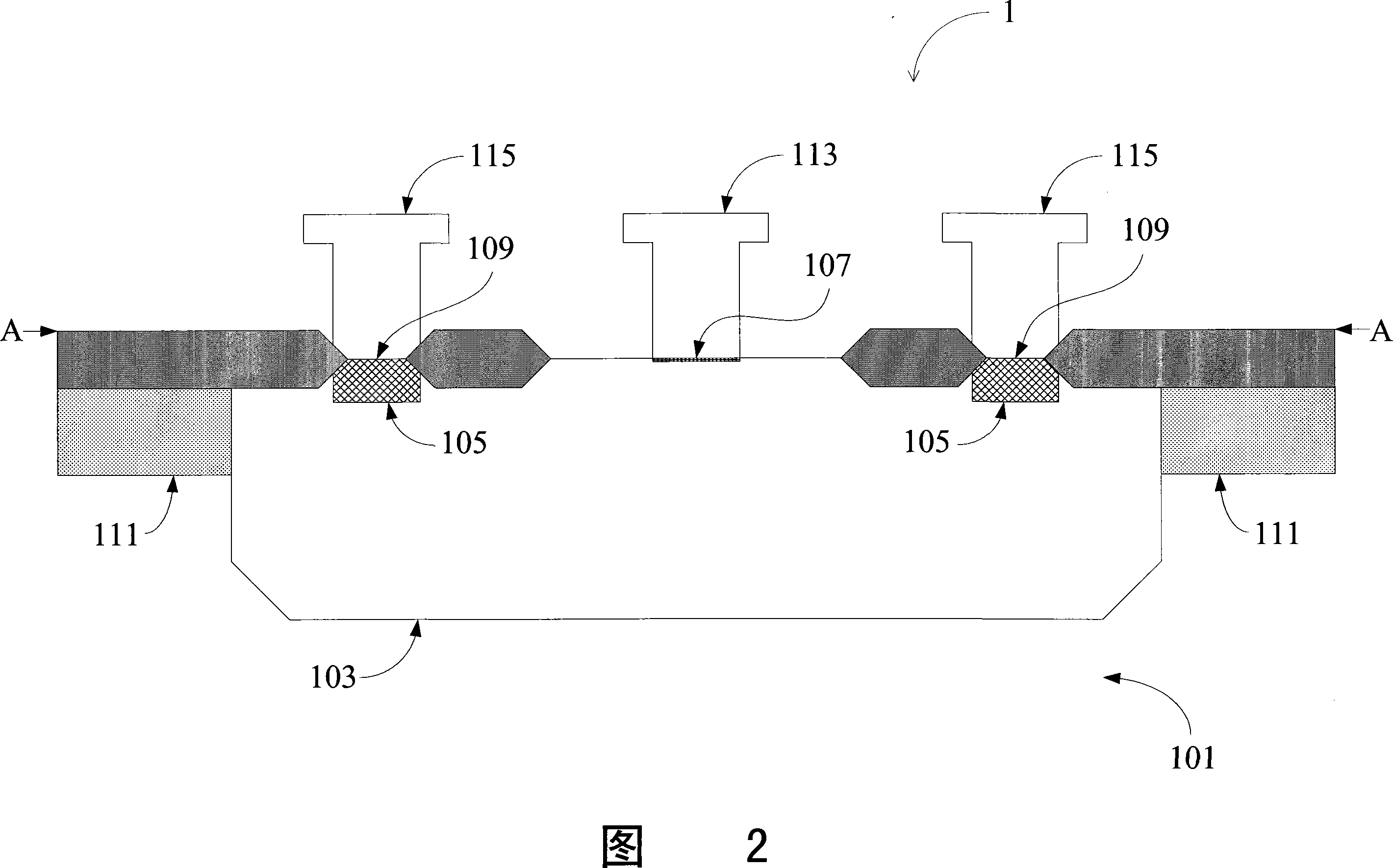
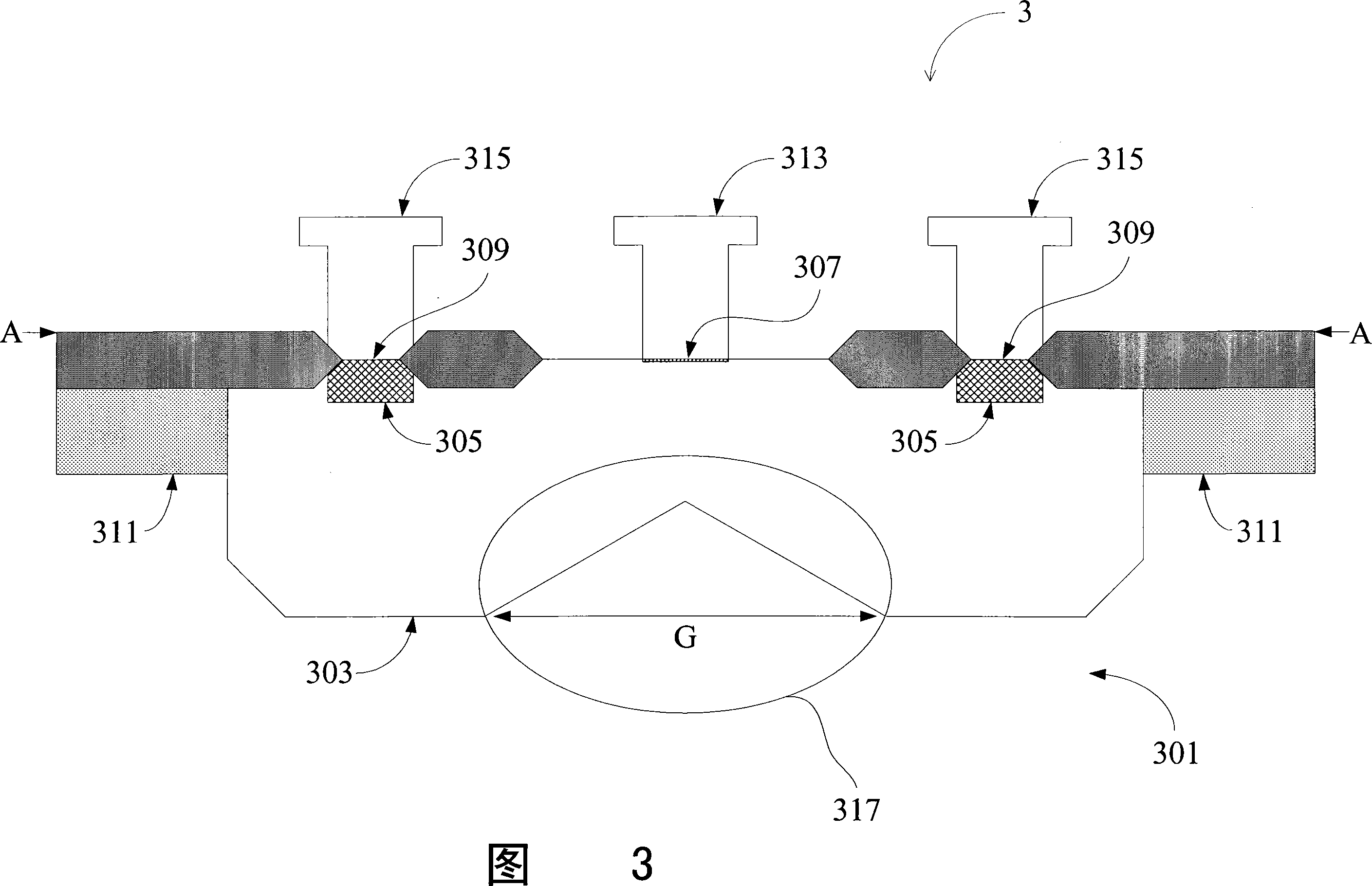
[0016] According to the first embodiment, the P-type substrate 301 is doped with P-type ions, and the N-type deep well region 303 is doped with N-type ions and formed on the P-type substrate 301 . The heavily doped region 305 is heavily doped with N-type ions and formed in the N-type deep well region 303 . The Schottky junction 307 contacts the Schottky electrode 313 with the N-type deep well region 303 . Ohmic junction 309 contacts ohmic electrode 315 with heavily doped region 305 . And the N-type deep well region 303 also has a geometric notch formed in a notch region 317 and has a lateral dimension G. As shown in FIG. The geometric notch region 317 is formed under the Schottky junction 307 , and the lateral dimension G can be used to adjust the breakdown voltage of the Schottky device 3 .

[0017] The second embodiment of the present invention is another Schottky device 4 shown in FIG. 4 and FIG. 5 . FIG. 4 is a top view showing the Schottky device 4 , and FIG. 5 is a pa...


PUM


Abstract

The present invention provides a Schottky element and its semiconductor manufacturing process. The Schottky element comprises a substrate, a deep well, a Schottky contact, and an Ohmic contact. The substrate is doped with type I ion. The deep well zone is doped with type II ion and formed in the substrate. The Schottky contact contacts a first electrode with the deep well. The Ohmic contact contacts a second electrode with a heavily doped zone containing type II ion in the deep well. Wherein, the deep well zone has a geometry gap formed under the Schottky and containing a transverse size, the type I ion and the type II ion are complemented, and the transverse size is for adjusting the electric breakdown strength.

Description

technical field [0001] The present invention relates to a Schottky element and a semiconductor process for manufacturing the Schottky element; more specifically, it relates to a semiconductor process for manufacturing a Schottky element with a high breakdown voltage. Background technique [0002] Schottky elements are widely used in many semiconductor circuits. Please refer to FIG. 1 and FIG. 2. FIG. 1 is a top view of a conventional Schottky element 1, and FIG. 2 shows a partial side view of the Schottky element 1 taken along the section line A-A of FIG. 1. Sectional view. Schottky element 1 includes a P-type substrate 101, an N-type deep well region 103, a heavily doped region 105 doped with N-type ions, a Schottky junction (contact) 107, an Ohmic (Ohmic) junction surface 109 , a doped region 111 doped with P-type ions, a Schottky electrode 113 and an ohmic electrode 115 . The Schottky junction 107 makes the Schottky electrode 113 contact with the N-type deep well regio...

Claims


Application Information

Patent Timeline
Patent Type & Authority Applications(China)
IPC IPC(8): H01L29/872H01L21/329
CPCH01L29/872H01L29/0692
Inventor 蒋秋志黄志丰伍佑国林隆世
Owner SYST GEN
Why Eureka
Try Eureka