

Display device induction structure and producing method thereof
A manufacturing method and a technology of a display device, which are applied in static indicators, nonlinear optics, instruments, etc., can solve the problems affecting liquid crystal gap support, uneven display brightness, unfavorable application and development of touch-sensitive flat-panel display devices, etc., and achieve The effect of solving poor response rate and reducing production cost
- Summary
- Abstract
- Description
- Claims
- Application Information
AI Technical Summary
Problems solved by technology
Method used
Image

Examples
Embodiment Construction
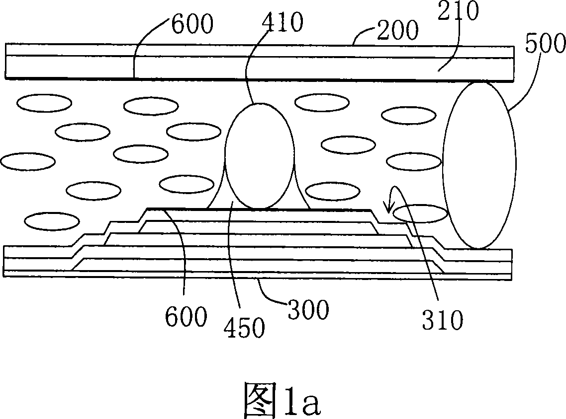
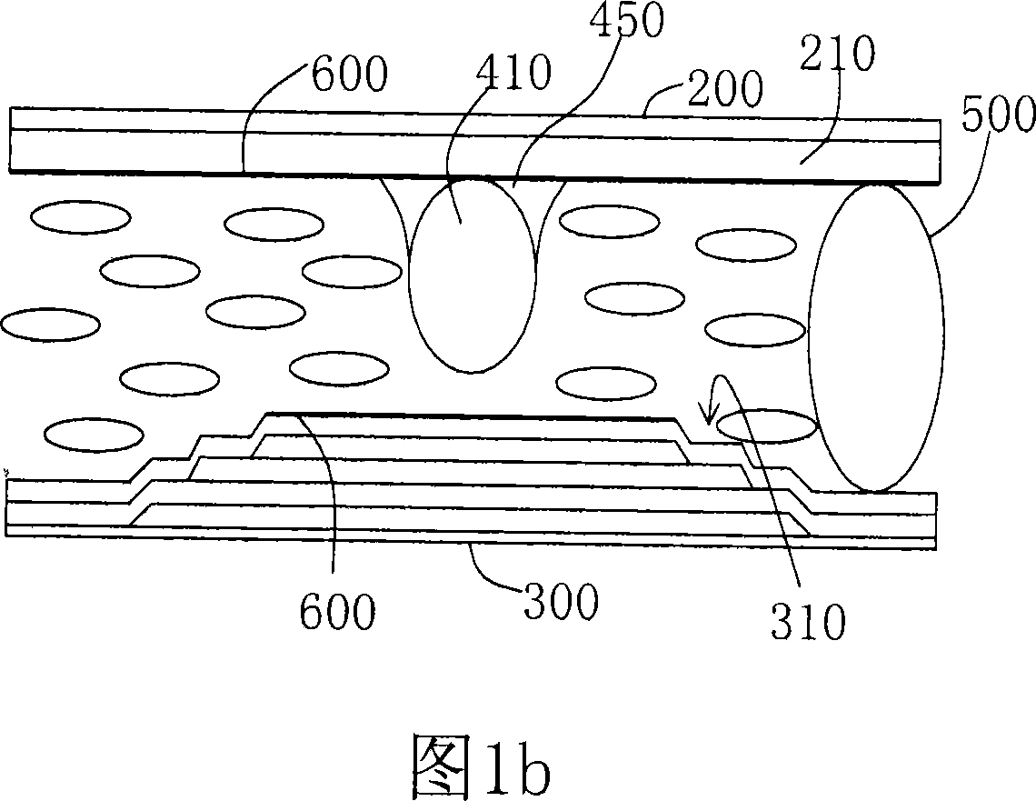
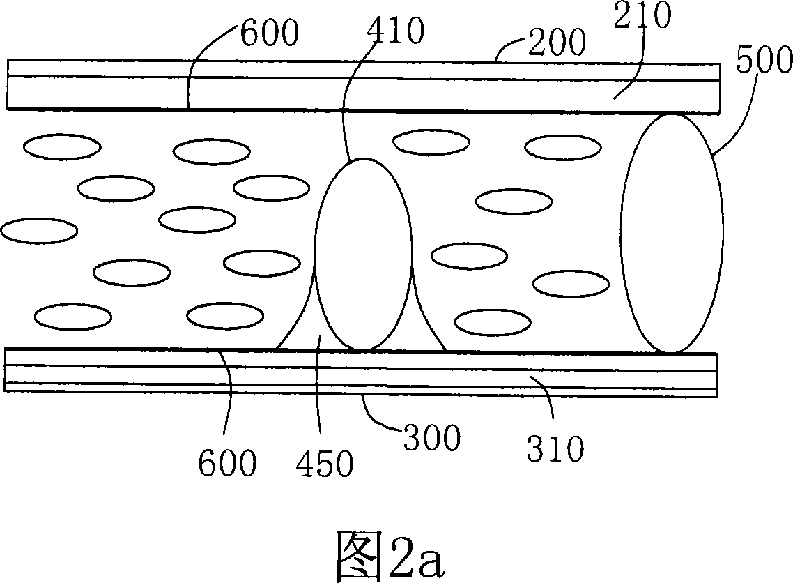
[0028] The present invention provides a sensing structure of a display device and a manufacturing method thereof. A spacer and a sensing bump (bump) are arranged on a touch panel liquid crystal gap (Cell gap) to form a sensing area (Sensor) by using fixed-point configuration technology. area). In the sensing structure of the display device and the manufacturing method thereof of the present invention, it is preferable to arrange conductive particles between the substrates to form sensing bumps and sensing regions by using fixed-point arrangement technology. The conductive particles applied to the sensing structure of the display device of the present invention preferably include but are not limited to metal particles or particles coated with indium tin oxide (ITO), that is, all conductive particles that can conduct between the sensing structures , all belong to the so-called conductive particles of the present invention. The "fixed-point configuration technology" mentioned he...
PUM
 Abstract
Description
Claims
Application Information