Solid-state image pickup device and mask manufacturing method

A technology of a solid-state imaging device and a manufacturing method, which is applied in the direction of electric solid-state devices, optics, optical elements, etc., can solve the problems of reduced light concentration and small spacing, and achieve the effect of improving the light concentration

Inactive Publication Date: 2007-11-28
PANASONIC CORP
View PDF2 Cites 4 Cited by
  • Summary
  • Abstract
  • Description
  • Claims
  • Application Information

AI Technical Summary

Problems solved by technology

[0009] However, conventional solid-state imaging devices have such a problem. Since the microlenses are arranged at a pitch smaller than that of the light-receiving part, and the farther away from the center, the more they are arranged toward the center. Therefore, the incident angle is the opposite, and the image height corresponds to When the incident angle characteristics are not proportional to the image height, it will reduce the light-gathering efficiency

Method used


Image

  • Solid-state image pickup device and mask manufacturing method
  • Solid-state image pickup device and mask manufacturing method
  • Solid-state image pickup device and mask manufacturing method

Examples


Embodiment approach 1

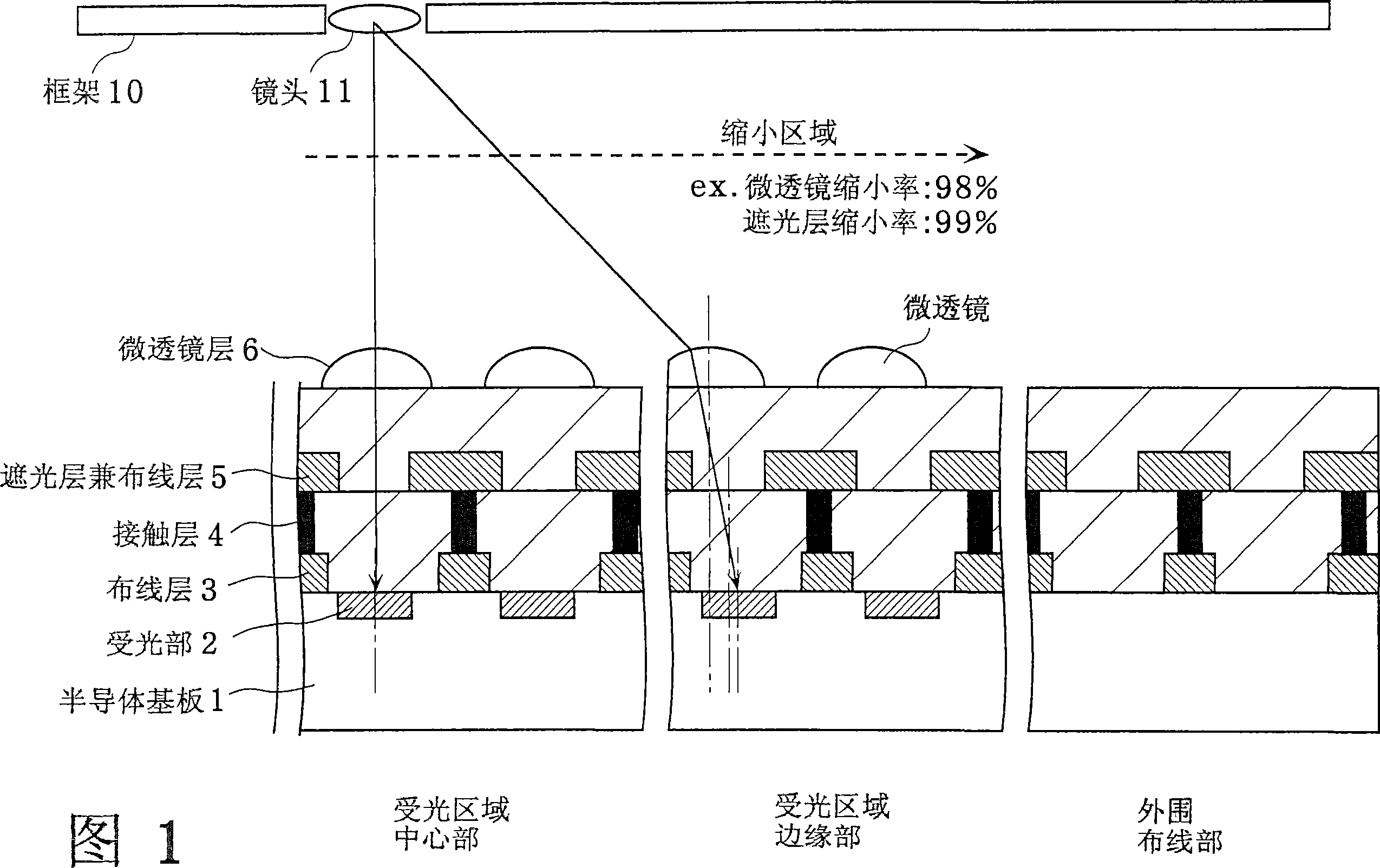
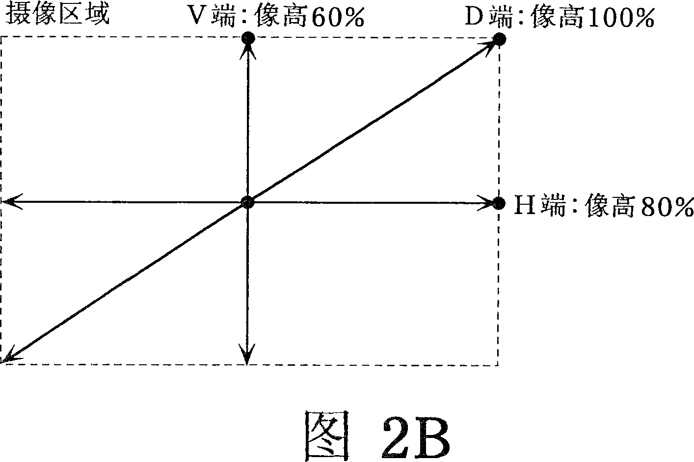
[0052]3A is a schematic diagram showing a plan view of the solid-state imaging device according to Embodiment 1 of the present invention. As shown in FIG. 3A , the surface of the solid-state imaging device roughly includes a light receiving area and a peripheral circuit area. The light-receiving area is composed of imaging areas 1 , 2 , and 3 , which are a plurality of areas. Each imaging area is divided by a quadrangular boundary whose center is the center of the optical axis (or optical center). In addition, the imaging areas 1, 2, and 3 may be divided by polygonal boundaries instead of quadrangular boundaries, or may be divided by circular boundaries centered on the center of the optical axis as shown in FIG. 3B.

[0053] FIG. 4 is a cross-sectional view showing the solid-state imaging device. This figure corresponds to the state in which four pixels near the boundary between imaging area 1 and imaging area 2 are arranged as shown in FIG. 3B or FIG. 3A , and the left side...

Embodiment approach 2

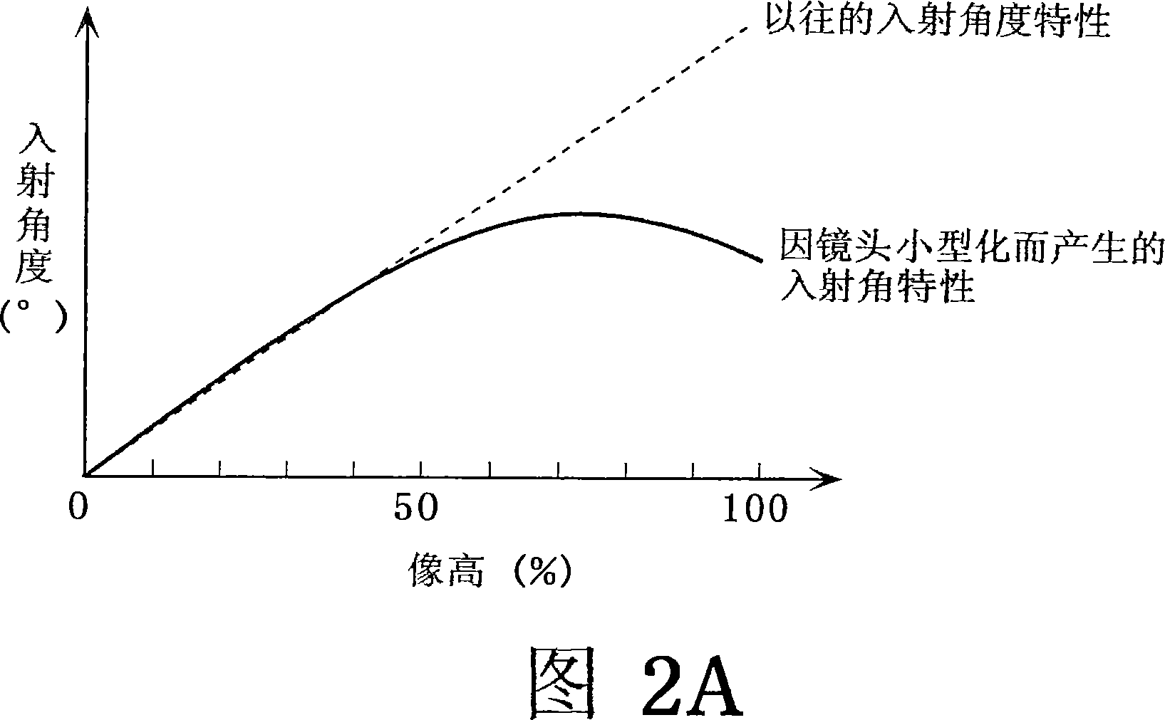
[0062] 7 is a cross-sectional view showing a solid-state imaging device according to Embodiment 2. FIG. In the same figure, the difference from the cross-section of the solid-state imaging device shown in FIG. The distance between them is L2, and the size of the opening is S2. The incident angle characteristics shown in FIG. 6A and FIG. 6B are the same. The description of the similarities will be omitted, and the description will focus on the differences. L1 and L2 are set to optimal values ​​according to the incident angle characteristics of the imaging areas 1 and 2 . In this example, it is assumed that L2>L1, L12>L1, and L12>=L2. That is, the pitch of the openings in the imaging area 1 is smaller than the pitch in the imaging area 2 . The size of the openings and the distance between the openings are also different. This means that the reduction ratio is different for each imaging area. Since the reduction ratio is different for each imaging area, the pitch of the ope...


PUM


Abstract

A solid-state image pickup device is provided with a light receiving region composed of photoelectric conversion elements two-dimensionally arranged, and a microlens layer composed of a microlens for introducing incoming light into the photoelectric conversion elements. The microlens layer is provided with a plurality of regions having different microlens pitches, at least one region includes a plurality of microlenses, and the pitch of the microlenses is different from the pitch of the photoelectric conversion elements.

Description

technical field [0001] The present invention relates to a solid-state imaging device having a light-receiving region composed of two-dimensionally arranged photoelectric conversion elements and microlenses corresponding to each photoelectric conversion element, and more particularly to a solid-state imaging device having a microlens layer composed of microlenses. The microlenses are arranged at a position deviated from the position directly above the photoelectric conversion element toward the optical center of the light receiving region. Background technique [0002] FIG. 1 is a cross-sectional view showing a conventional solid-state imaging device disclosed, for example, in Patent Document 1 or the like. In this figure, the central part of the light receiving area, the edge part in the light receiving area, and a part of the peripheral wiring part outside the light receiving area of ​​the solid-state imaging device are respectively shown. This solid-state imaging device i...

Claims


Application Information

Patent Timeline
Patent Type & Authority Applications(China)
IPC IPC(8): H01L27/14G02B3/00
CPCH01L27/14621H01L27/14632H01L27/14623H01L27/14627G02B3/00H01L27/14
Inventor 桝山雅之植田敦
Owner PANASONIC CORP
Why Eureka
Try Eureka