Architecture for general purpose programmable semiconductor processing system and methods therefor

A technology for processing systems and semiconductors, applied in general control systems, semiconductor/solid-state device manufacturing, control/regulation systems, etc.

Active Publication Date: 2008-02-13
LAM RES CORP
View PDF0 Cites 3 Cited by
  • Summary
  • Abstract
  • Description
  • Claims
  • Application Information

AI Technical Summary

Problems solved by technology

This process can take weeks and potentially cost hundreds of thousands of dollars

Method used


Image

  • Architecture for general purpose programmable semiconductor processing system and methods therefor
  • Architecture for general purpose programmable semiconductor processing system and methods therefor
  • Architecture for general purpose programmable semiconductor processing system and methods therefor

Examples


Embodiment Construction

[0017] The invention will now be described in detail with reference to several preferred embodiments as shown in the accompanying drawings. In the following description, numerous specific details are set forth in order to provide a thorough understanding of the present invention. It will be apparent, however, to one skilled in the art that the present invention may be practiced without some or all of these specific details. In other instances, well known process steps and / or structures have not been described in detail so as not to obscure the present invention.

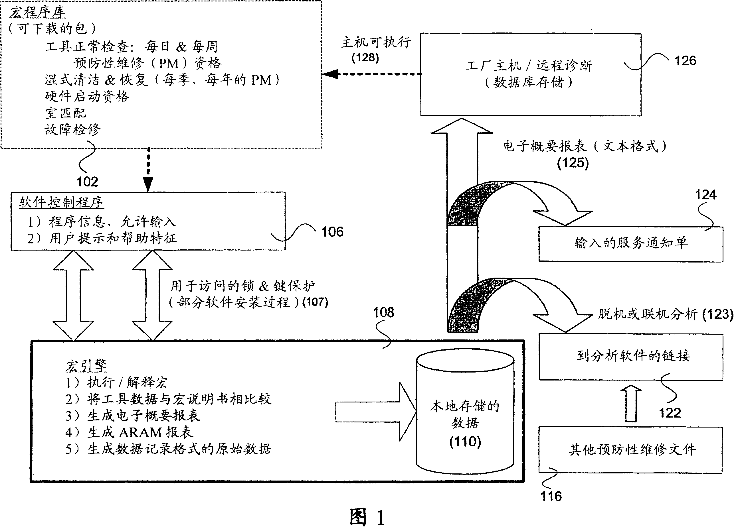
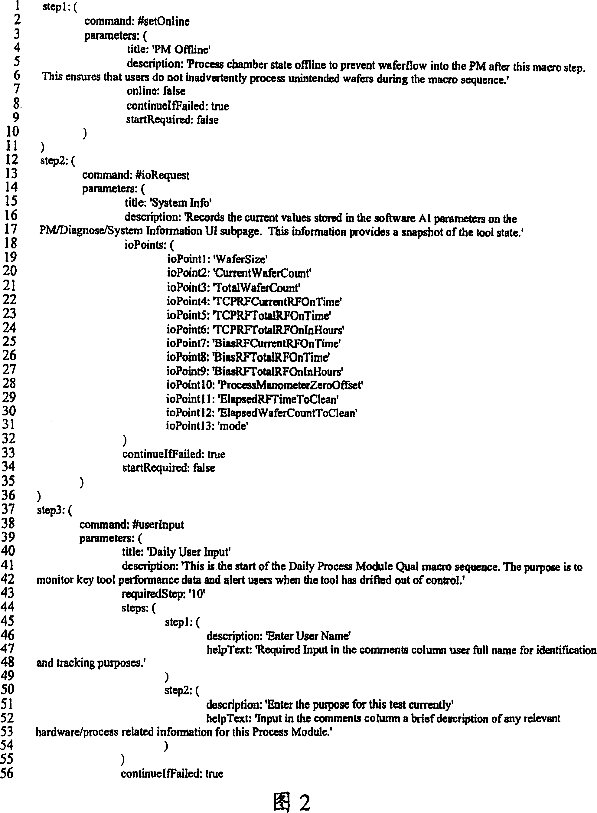
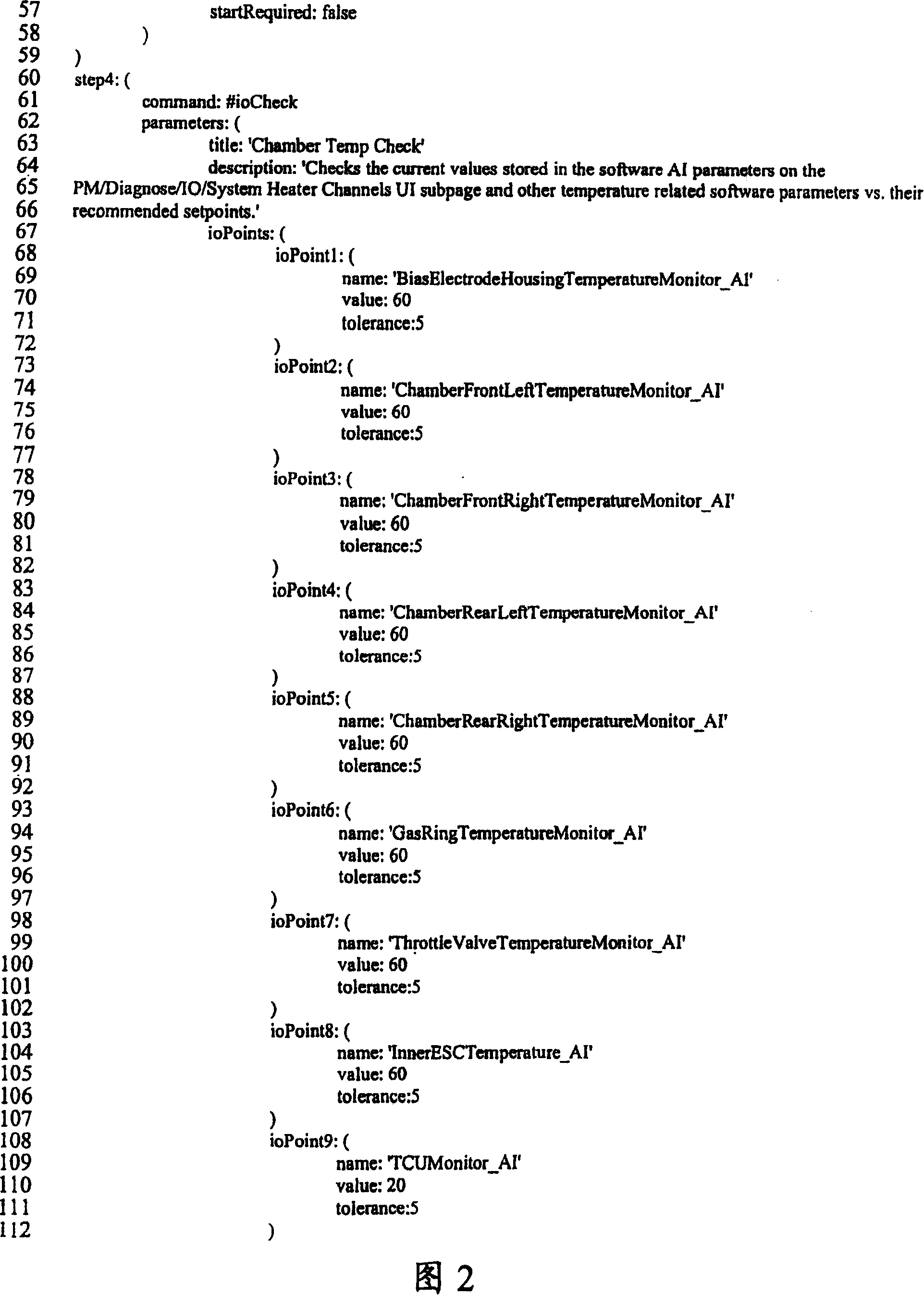
[0018] According to one embodiment of the present invention, a macro engine is advantageously used to extend and enhance the performance of a semiconductor processing system. In other words, a set of control instructions or steps called macros can be created to control the functions of the semiconductor processing system and further store processing information in memory to generate reports. Furthermore, these inst...


PUM


Abstract

The present invention relates to a cosmetic applicator, in particular for applying nail varnish or mascara, the applicator including at least two applicator elements each presenting at least one periodic pattern with at least one undulation, at least two periodic patterns being different.

Description

technical field [0001] The present invention relates generally to semiconductor manufacturing technology and, more particularly, to methods and apparatus for optimizing a set of operations in a semiconductor capital equipment processing system. Background technique [0002] Hundreds of millions of dollars are often spent designing and operating semiconductor manufacturing equipment. Optimizing throughput and reducing costs are therefore critical to profitability. However, the basic equipment handling systems within these devices often require considerable human intervention, which can create the potential for process variances and even outright operational errors. [0003] Most semiconductor basic device processing systems are typically controlled by a sophisticated computer including an operating software program in which the user is provided via an interface the ability to send requests to the device and receive output information from the device. These process steps are...

Claims


Application Information

Patent Timeline
Patent Type & Authority Applications(China)
IPC IPC(8): G06F19/00H01L
CPCG05B19/418G05B2219/32128G05B2219/35262H01L21/67276G05B2219/45031Y02P90/02Y02P90/80G06F9/00
Inventor 罗杰·帕特里克文森特·翁黄仲镐
Owner LAM RES CORP
Why Eureka
Try Eureka