Semiconductor device, power supply device, and information processing device

A semiconductor and voltage technology, used in semiconductor devices, semiconductor/solid-state device manufacturing, output power conversion devices, etc., can solve problems such as large circuit area, low efficiency, and inability to form body diodes, and achieves reduction of potential difference. The effect of preventing poor operation

Inactive Publication Date: 2008-04-30
ROHM CO LTD
View PDF2 Cites 12 Cited by
  • Summary
  • Abstract
  • Description
  • Claims
  • Application Information

AI Technical Summary

Problems solved by technology

However, this approach requires multiple switch
Therefore, a large circuit area is required
Also, this method uses series-connected MOS transistors, so there is a high on-state resistance across the MOS transistors in the steady output state, resulting in inefficiency
[0004] Another approach shown in Figure 10 is to connect the back gate of the MOS transistor 910 to the reference potential so that the body diode BD cannot be formed

Method used


Image

  • Semiconductor device, power supply device, and information processing device
  • Semiconductor device, power supply device, and information processing device
  • Semiconductor device, power supply device, and information processing device

Examples


Embodiment Construction

[0071] First, a first embodiment of the present invention is described.

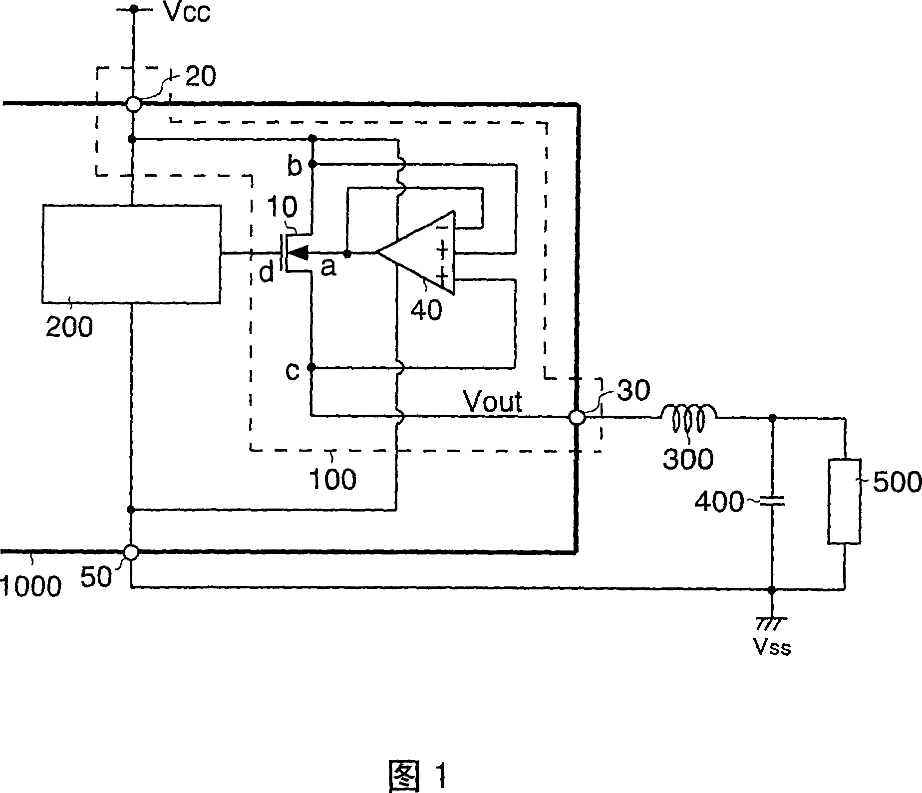
[0072] FIG. 1 shows a power supply device using a semiconductor device according to the present invention as a first embodiment.

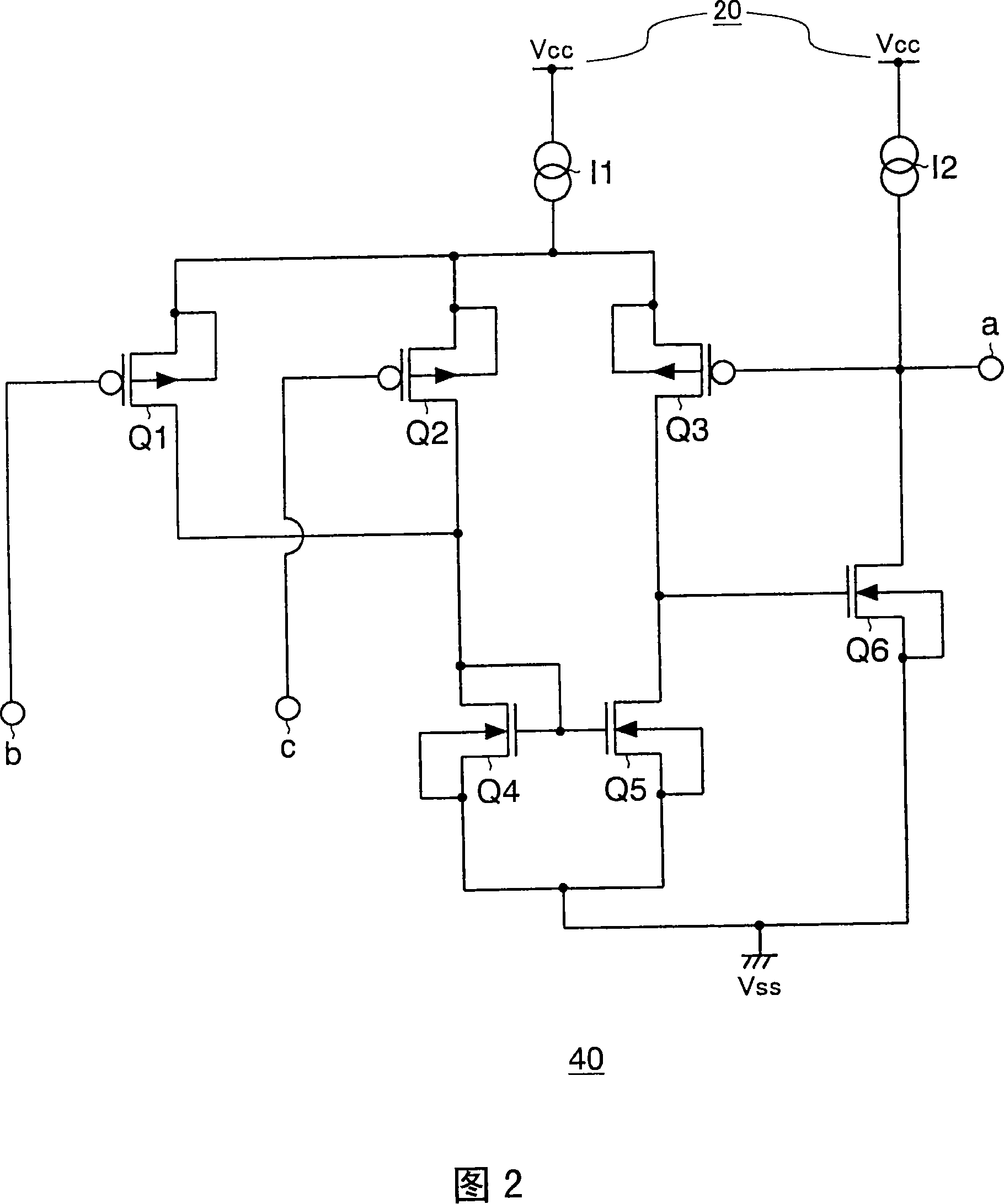
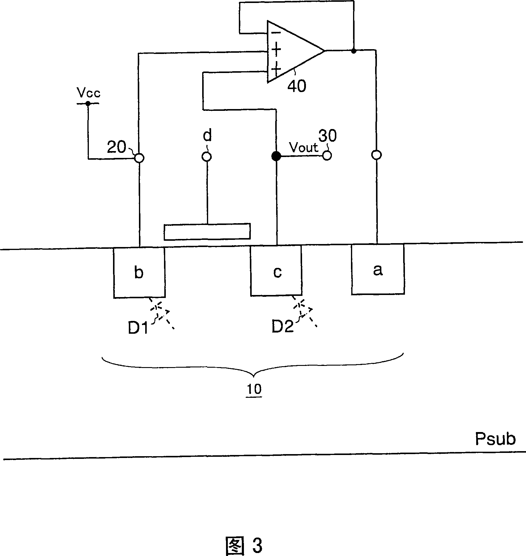
[0073] As shown in FIG. 1 , the semiconductor device 100 of this embodiment constitutes a part of a semiconductor device 1000 . The semiconductor device 100 is composed of a MOS transistor 10 having a back gate terminal "a", a first region "b" serving as one of a source region and a drain region, and a first region "b" serving as a source region and a drain region. The second region "c" of the other of the drain regions; the input terminal 20, which is connected to the first region "b", and, for example, a power supply voltage Vcc as an input voltage is applied to the input terminal from the outside of the semiconductor device 1000 an output terminal 30 which is connected to the second region "c" and from which the output voltage Vout is output outside the semiconductor devi...


PUM


Abstract

A semiconductor device (100) includes a MOS transistor (10) having a back gate region ''a'', a first region ''b'' serving as one of a source region and a drain region, and a second region ''c'' serving as the other of the source region and the drain region. The semiconductor device further includes an input terminal (20) connected to the first region ''b'' and to which an input voltage is applied from outside the semiconductor device (100), an output terminal (30) connected to the second region ''c'' and outputting an output voltage outside the semiconductor device (100), and a back gate control circuit (40) for applying the input voltage or the output voltage to the back gate region ''a''. With this configuration of the semiconductor device having the output MOS transistor, even when a reverse bias is applied between the input and the output terminal, the terminals are insulated from each other and lowering of the drain current by the substrate bias effect can be suppressed.

Description

technical field [0001] The present invention relates to a semiconductor device using a MOS transistor as an output device. Background technique [0002] As shown in FIG. 9 , a conventional power supply device outputs a desired output voltage via an output terminal 30 by turning on and off the gate of an output MOS transistor 900 . Here, between the source region and the drain region of the output MOS transistor 900, there generally exists a body diode BD as a parasitic device. Thus, if for some reason a reverse bias is applied between the input terminal 20 and the output terminal 30, the current will flow between the source and the drain through the body diode BD and this makes it impossible to Insulation between the region and the drain region. [0003] In Patent Document 1 listed below, a method of overcoming the above-mentioned problems due to the presence of the body diode BD is disclosed. However, this approach requires multiple switches. Therefore, a large circuit ...

Claims


Application Information

Patent Timeline
Patent Type & Authority Applications(China)
IPC IPC(8): H01L21/822H01L21/8234H01L27/04H01L27/088H02M3/155
CPCH01L27/0266H01L21/823481H02M3/156H01L21/761
Inventor 梅本清贵
Owner ROHM CO LTD
Why Eureka
Try Eureka