Three-dimensional configurations providing electromagnetic interference shielding for electronics enclosures
一种电磁干扰屏蔽、电子设备的技术,应用在磁场/电场屏蔽、屏蔽材料、电气元件等方向,能够解决昂贵、耐受性差等问题,达到充分EMI屏蔽、廉价屏蔽解决方案的效果
- Summary
- Abstract
- Description
- Claims
- Application Information
AI Technical Summary
Problems solved by technology
Method used
Image
Examples
Embodiment Construction
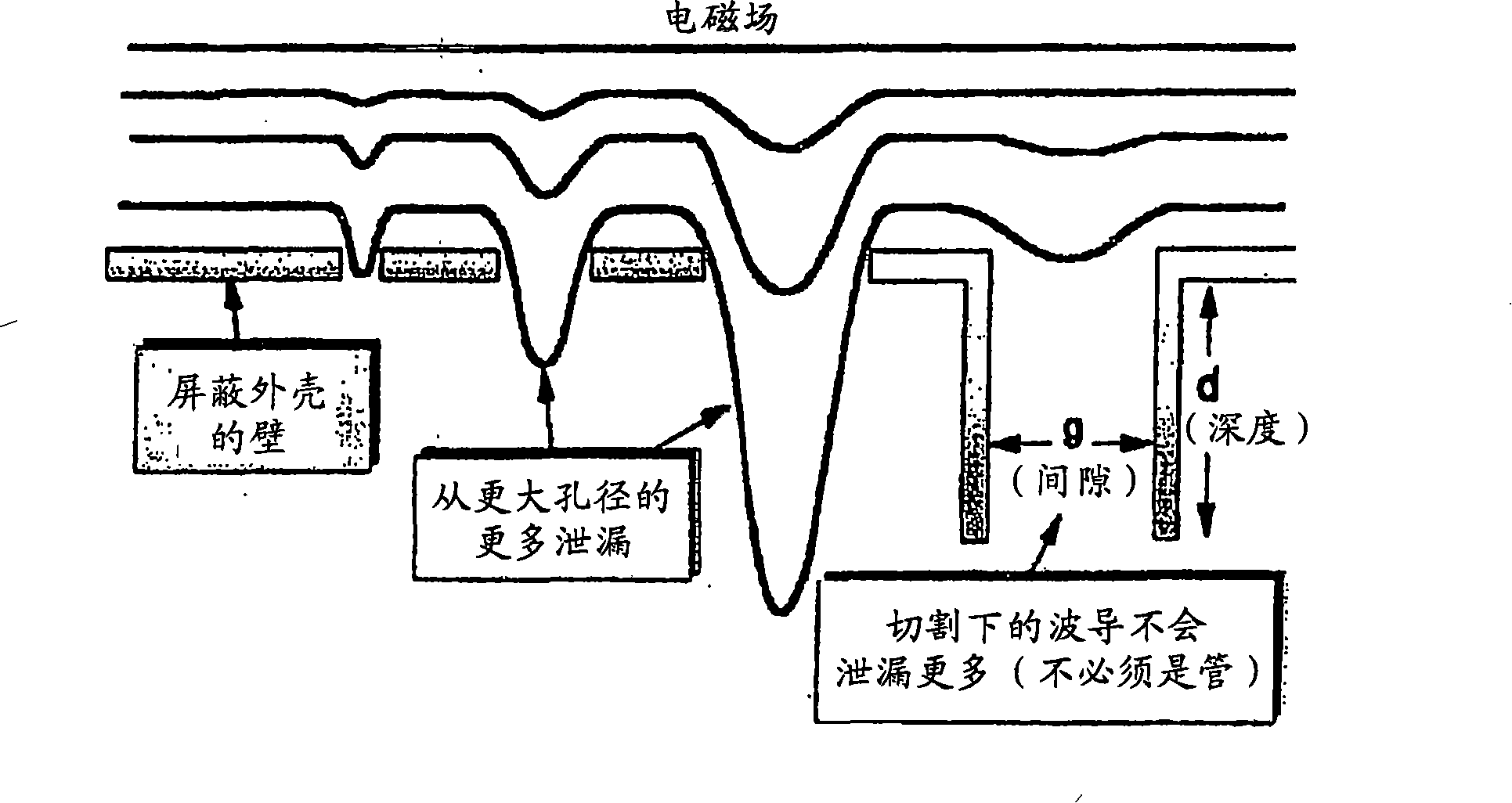
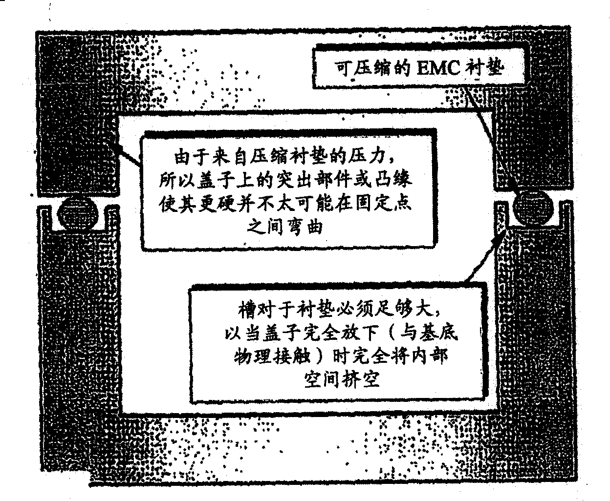
[0088] Utilizing the "shell" or "scallop" embodiment of the invention as shown in Figures 5A and 5B, three-dimensional shapes can be formed or otherwise configured such that they generally extend along the inner perimeter of the edge and the two parts FSE and FL come together in together, and satisfy the "sinusoid". All that is necessary to implement the 3D implementation of the invention is to "cut" or stamp the edges of the metal, and do the same cuts, and they come together in a "30 gap" or something like that. Advantages of the basic embodiment of the invention include, inter alia, the fact that no contacts are required and thus do not deteriorate over time (see FIG. 9B ). It is not necessary for the FSE and FL parts to make physical contact. Further advantages include the absence of tolerances and the absence of deformation.
[0089] Referring again to FIG. 5A , a first embodiment of a three-dimensional EMI shielding solution for electronic device enclosures is shown in...
PUM
 Abstract
Description
Claims
Application Information


